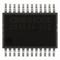
CS5534-BSZ Cirrus Logic Inc, CS5534-BSZ Datasheet - Page 39

CS5534-BSZ
Manufacturer Part Number
CS5534-BSZ
Description
IC ADC 24BIT 4CH W/LNA 20SSOP
Manufacturer
Cirrus Logic Inc
Specifications of CS5534-BSZ
Number Of Converters
1
Package / Case
24-SSOP
Number Of Bits
24
Sampling Rate (per Second)
3.84k
Data Interface
Serial
Power Dissipation (max)
45mW
Voltage Supply Source
Analog and Digital, Dual ±
Operating Temperature
-40°C ~ 85°C
Mounting Type
Surface Mount
Number Of Adc Inputs
4
Architecture
Delta-Sigma
Conversion Rate
6.25 SPs to 3840 SPs
Resolution
24 bit
Input Type
Voltage
Interface Type
Serial (3-Wire)
Voltage Reference
2.5 V
Maximum Power Dissipation
500 mW
Maximum Operating Temperature
+ 85 C
Mounting Style
SMD/SMT
Minimum Operating Temperature
- 40 C
Lead Free Status / RoHS Status
Lead free / RoHS Compliant
For Use With
598-1016 - EVAL BOARD FOR CS5534
Lead Free Status / Rohs Status
Lead free / RoHS Compliant
Other names
598-1116-5
Available stocks
Company
Part Number
Manufacturer
Quantity
Price
Company:
Part Number:
CS5534-BSZ
Manufacturer:
Qorvo
Quantity:
10
Company:
Part Number:
CS5534-BSZ
Manufacturer:
CIRRUS
Quantity:
676
Part Number:
CS5534-BSZ
Manufacturer:
CIRRUS
Quantity:
20 000
2.10. Clock Generator
The CS5531/32/33/34 include an on-chip inverting
amplifier which can be connected with an external
crystal to provide the master clock for the chip. Fig-
ure 20 illustrates the on-chip oscillator. It includes
loading capacitors and a feedback resistor to form
a Pierce oscillator configuration. The chips are de-
signed to operate using a 4.9152 MHz crystal;
however, other crystals with frequencies between
1 MHz to 5 MHz can be used. One lead of the crys-
tal should be connected to OSC1 and the other to
OSC2. Lead lengths should be minimized to reduce
stray capacitance. Note that while using the on-chip
oscillator, neither OSC1 or OSC2 is capable of di-
rectly driving any off-chip logic. When the on-chip
oscillator is used, the voltage on OSC2 is typically
0.5 V peak-to-peak. This signal is not compatible
with external logic unless additional external cir-
cuitry is added. The OSC2 output should be used if
the on-chip oscillator output is used to drive other
circuitry.
The designer can use an external CMOS-compati-
ble oscillator to drive OSC2 with a 1 MHz to
5 MHz clock for the ADC. The external clock into
OSC2 must overdrive the 60 µA output of the on-
chip amplifier. This will not harm the on-chip cir-
cuitry. In this scheme, OSC1 should be left uncon-
nected.
DS289F5
OSC1
20 pF
Figure 20. On-chip Oscillator Model
1 MΩ
~ ~ 60 µA
20 pF
2.11. Power Supply Arrangements
The CS5531/32/33/34 are designed to operate from
single or dual analog supplies and a single digital
supply. The following power supply connections
are possible:
VA+ = +5V; VA- = 0V; VD+ = +3V to +5V
VA+ = +2.5V; VA- = -2.5V; VD+ = +3V to +5V
VA+ = +3V; VA- = -3V; VD+ = +3V
A VA+ supply of +2.5 V, +3.0 V, or +5.0 V should
be maintained at ±5% tolerance. A VA- supply of
-2.5 V or -3.0 V should be maintained at ±5% tol-
erance. VD+ can extend from +2.7 V to +5.5 V
with the additional restriction that:
[(VD+) - (VA-)] < 7.5 V.
Figure 21 illustrates the CS5532 connected with a
single +5.0 V supply to measure differential inputs
relative to a common mode of 2.5 V. Figure 22 il-
lustrates the CS5532 connected with ±2.5 V bipo-
lar analog supplies and a +3 V to +5 V digital
supply to measure ground referenced bipolar sig-
nals. Figures 23 and 24 illustrate the CS5532 con-
nected with ±3 V analog supplies and a +3 V
digital supply to measure ground-referenced bipo-
lar signals.
Figure 25 illustrates alternate bridge configurations
which can be measured with the converter. Voltage
V1 can be measured with the PGIA gain set to 1x
as the input amplifier on this gain setting can go
rail-to-rail. Voltage V2 should be measured with
the PGIA gain set at 2x or higher as the instrumen-
V
TH
OSC2
+
-
NOTE: 20 pF capacitors are on
chip and should not be added
externally.
CS5531/32/33/34-AS
MCLK
39


