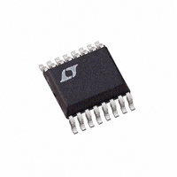
LTC1867LIGN#PBF Linear Technology, LTC1867LIGN#PBF Datasheet - Page 8

LTC1867LIGN#PBF
Manufacturer Part Number
LTC1867LIGN#PBF
Description
IC ADC 16BIT 8CH 175KSPS 16SSOP
Manufacturer
Linear Technology
Datasheet
1.LTC1863LCGNPBF.pdf
(16 pages)
Specifications of LTC1867LIGN#PBF
Number Of Bits
16
Sampling Rate (per Second)
175k
Data Interface
MICROWIRE™, Serial, SPI™
Number Of Converters
1
Power Dissipation (max)
2.7mW
Voltage Supply Source
Single Supply
Operating Temperature
-40°C ~ 85°C
Mounting Type
Surface Mount
Package / Case
16-SSOP (0.150", 3.90mm Width)
Number Of Elements
1
Resolution
16Bit
Architecture
SAR
Sample Rate
175KSPS
Input Polarity
Unipolar/Bipolar
Input Type
Voltage
Rated Input Volt
2.5/±1.25V
Differential Input
Yes
Power Supply Requirement
Analog and Digital
Single Supply Voltage (typ)
3.3V
Single Supply Voltage (min)
2.7V
Single Supply Voltage (max)
3.6V
Dual Supply Voltage (typ)
Not RequiredV
Dual Supply Voltage (min)
Not RequiredV
Dual Supply Voltage (max)
Not RequiredV
Power Dissipation
2.7mW
Differential Linearity Error
-2LSB(Min)
Integral Nonlinearity Error
±4LSB
Operating Temp Range
-40C to 85C
Operating Temperature Classification
Industrial
Mounting
Surface Mount
Pin Count
16
Package Type
SSOP N
Lead Free Status / RoHS Status
Lead free / RoHS Compliant
Available stocks
Company
Part Number
Manufacturer
Quantity
Price
LTC1863L/LTC1867L
TYPICAL CONNECTION DIAGRAM
TEST CIRCUITS
TIMING DIAGRAMS
8
CS/CONV
CS/CONV
CS/CONV
SDO
(A) Hi-Z TO V OH AND V OL TO V OH
SCK
SDO
Load Circuits for Access Timing
t
t
4
7
Hi-Z
3k
(SDO Valid After CS/CONV↓)
(SLEEP Mode Wake-Up Time)
t
1
50%
(For Short Pulse Mode)
SLEEP BIT (SLP = 0)
READ-IN
50%
C
L
0.45V
t
1
(B) Hi-Z TO V OL AND V OH TO V OL
t
4
t
7
SDO
2.7V
50%
1.9V
0.45V
3k
C
SINGLE-ENDED
DIFFERENTIAL
L
1863L7L TC01
INPUTS
±1.25V
INPUT
1863L7L TD01c
2.5V
1863L7L TD01e
1863L7L TD01a
50%
+
–
+
CH0
CH1
CH2
CH3
CH4
CH5
CH6
CH7/COM
LTC1863L/
LTC1867L
REFCOMP
CS/CONV
GND
V
SDO
V
SCK
SDI
REF
DD
CS/CONV
SCK
SDO
SDI
DIGITAL
I/O
10μF
10μF
2.5V
t
2.7V TO 3.6V
SDO
3
SCK
Load Circuits for Output Float Delay
(SDO Valid Hold Time After SCK↓)
t
5
t
t
SDO
6
2
(SDI Setup Time Before SCK↑)
t
1.9V
0.45V
1863L7L TCD
2.2μF
(SDI Hold Time After SCK↑)
(SDO Valid After SCK↓)
8
1.9V
1.25V
(A) V OH TO Hi-Z
(BUS Relinquish Time)
t
8
3k
t
5
90%
10%
C
L
1.9V
SDO
t
6
(B) V OL TO Hi-Z
2.7V
0.45V
1863L7L TC02
0.45V
1.9V
3k
t
1863L7L TD01b
t
3
C
2
Hi-Z
L
1.9V
0.45V
1863L7L TD01d
1863L7L TD01f
1863l7lfc


