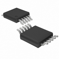
LTC2411IMS#PBF Linear Technology, LTC2411IMS#PBF Datasheet - Page 15

LTC2411IMS#PBF
Manufacturer Part Number
LTC2411IMS#PBF
Description
IC A/D CONV 24BIT MICRPWR 10MSOP
Manufacturer
Linear Technology
Datasheet
1.LTC2411CMSPBF.pdf
(40 pages)
Specifications of LTC2411IMS#PBF
Number Of Bits
24
Sampling Rate (per Second)
7.5
Data Interface
MICROWIRE™, Serial, SPI™
Number Of Converters
2
Power Dissipation (max)
1mW
Voltage Supply Source
Single Supply
Operating Temperature
-40°C ~ 85°C
Mounting Type
Surface Mount
Package / Case
10-TFSOP, 10-MSOP (0.118", 3.00mm Width)
Number Of Elements
1
Resolution
24Bit
Architecture
Delta-Sigma
Sample Rate
0.008KSPS
Input Polarity
Bipolar
Input Type
Voltage
Rated Input Volt
±2.75V
Differential Input
Yes
Power Supply Requirement
Single
Single Supply Voltage (typ)
3.3/5V
Single Supply Voltage (min)
2.7V
Single Supply Voltage (max)
5.5V
Dual Supply Voltage (typ)
Not RequiredV
Dual Supply Voltage (min)
Not RequiredV
Dual Supply Voltage (max)
Not RequiredV
Integral Nonlinearity Error
14ppm of Vref
Operating Temp Range
-40C to 85C
Operating Temperature Classification
Industrial
Mounting
Surface Mount
Pin Count
10
Package Type
MSOP
Input Signal Type
Differential
Lead Free Status / RoHS Status
Lead free / RoHS Compliant
Available stocks
Company
Part Number
Manufacturer
Quantity
Price
APPLICATIO S I FOR ATIO
Table 3. LTC2411/LTC2411-1 State Duration
State
CONVERT
SLEEP
DATA OUTPUT
converter status and during the data output state it is used
to read the conversion result.
Serial Clock Input/Output (SCK)
The serial clock signal present on SCK (Pin 9) is used to
synchronize the data transfer. Each bit of data is shifted out
the SDO pin on the falling edge of the serial clock.
In the Internal SCK mode of operation, the SCK pin is an
output and the LTC2411/LTC2411-1 create their own se-
rial clock by dividing the internal conversion clock by 8. In
the External SCK mode of operation, the SCK pin is used
as input. The internal or external SCK mode is selected on
power-up and then reselected every time a HIGH-to-LOW
transition is detected at the CS pin. If SCK is HIGH or float-
ing at power-up or during this transition, the converter
enters the internal SCK mode. If SCK is LOW at power-up
or during this transition, the converter enters the external
SCK mode.
Serial Data Output (SDO)
The serial data output pin, SDO (Pin 8), provides the result
of the last conversion as a serial bit stream (MSB first)
during the data output state. In addition, the SDO pin is
Operating Mode
Internal Oscillator
External Oscillator
Internal Serial Clock
External Serial Clock with
Frequency f
U
SCK
U
kHz
W
F
(60Hz Rejection)
F
(50Hz Rejection)
F
(Simultaneous 50Hz/60Hz Rejection)
F
with Frequency f
(f
F
(Internal Oscillator)
F
(Internal Oscillator)
F
Frequency f
O
O
O
O
O
O
O
EOSC
= LOW (LTC2411)
= HIGH (LTC2411)
= LOW (LTC2411-1)
= External Oscillator
= LOW/HIGH (LTC2411)
= LOW (LTC2411-1)
= External Oscillator with
/2560 Rejection)
U
EOSC
EOSC
kHz
kHz
used as an end of conversion indicator during the conver-
sion and sleep states.
When CS (Pin 7) is HIGH, the SDO driver is switched to a
high impedance state. This allows sharing the serial
interface with other devices. If CS is LOW during the
convert or sleep state, SDO will output EOC. If CS is LOW
during the conversion phase, the EOC bit appears HIGH on
the SDO pin. Once the conversion is complete, EOC goes
LOW. The device remains in the sleep state until the first
rising edge of SCK occurs while CS = LOW.
Chip Select Input (CS)
The active LOW chip select, CS (Pin 7), is used to test the
conversion status and to enable the data output transfer as
described in the previous sections.
In addition, the CS signal can be used to trigger a new
conversion cycle before the entire serial data transfer has
been completed. The LTC2411/LTC2411-1 will abort any
serial data transfer in progress and start a new conversion
cycle anytime a LOW-to-HIGH transition is detected at the
CS pin after the converter has entered the data output state
(i.e., after the first rising edge of SCK occurs with
CS = LOW).
Duration
133ms, Output Data Rate 7.5 Readings/s
160ms, Output Data Rate 6.2 Readings/s
147ms, Output Data Rate 6.8 Readings/s
20510/f
As Long As CS = HIGH Until CS = LOW and SCK
As Long As CS = LOW But Not Longer Than 1.67ms
(32 SCK cycles)
As Long As CS = LOW But Not Longer Than 1.83ms
(32 SCK cycles)
As Long As CS = LOW But Not Longer Than 256/f
(32 SCK cycles)
As Long As CS = LOW But Not Longer Than 32/f
(32 SCK cycles)
EOSC
LTC2411/LTC2411-1
s, Output Data Rate f
EOSC
/20510 Readings/s
SCK
EOSC
ms
15
ms


