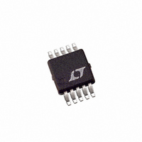
LTC1407CMSE-1#PBF Linear Technology, LTC1407CMSE-1#PBF Datasheet - Page 3

LTC1407CMSE-1#PBF
Manufacturer Part Number
LTC1407CMSE-1#PBF
Description
IC ADC 12BIT 3MSPS 10-MSOP
Manufacturer
Linear Technology
Datasheet
1.LTC1407CMSE-1PBF.pdf
(26 pages)
Specifications of LTC1407CMSE-1#PBF
Number Of Bits
12
Sampling Rate (per Second)
3M
Data Interface
Serial, SPI™
Number Of Converters
1
Power Dissipation (max)
14mW
Voltage Supply Source
Single Supply
Operating Temperature
0°C ~ 70°C
Mounting Type
Surface Mount
Package / Case
10-TFSOP, 10-MSOP (0.118", 3.00mm Width) Exposed Pad
Lead Free Status / RoHS Status
Lead free / RoHS Compliant
Available stocks
Company
Part Number
Manufacturer
Quantity
Price
DYNAMIC ACCURACY
ANALOG INPUT
otherwise specifi cations are at T
SYMBOL PARAMETER
V
V
I
C
t
t
t
t
CMRR
otherwise specifi cations are at T
CHO
SYMBOL PARAMETER
SINAD
THD
SFDR
IMD
IN
ACQ
AP
JITTER
SK
IN
CM
IN
–
/CH1
Signal-to-Noise Plus
Distortion Ratio
Total Harmonic
Distortion
Spurious Free
Dynamic Range
Intermodulation
Distortion
Code-to-Code
Transition Noise
Full Power Bandwidth V
Full Linear Bandwidth S/(N + D) ≥ 68dB
Analog Differential Input Range (Notes 3, 8, 9)
Analog Common Mode + Differential
Input Range (Note 10)
Analog Input Leakage Current
Analog Input Capacitance
Sample-and-Hold Acquisition Time
Sample-and-Hold Aperture Delay Time
Sample-and-Hold Aperture Delay Time Jitter
Sample-and-Hold Aperture Skew from CH0 to CH1
Analog Input Common Mode Rejection Ratio
–
= 1.5V DC. Differential signals drive both inputs of each channel with V
CONDITIONS
100kHz Input Signal (Note 19)
750kHz Input Signal (Note 19)
100kHz Input Signal, External V
V
750kHz Input Signal, External V
V
100kHz First 5 Harmonics (Note 19)
750kHz First 5 Harmonics (Note 19)
100kHz Input Signal (Note 19)
750kHz Input Signal (Note 19)
0.625V
into CH0
to CH1
V
DD
DD
REF
IN
The
A
A
= 2.5V
= 25°C. With internal reference, V
= 25°C. With internal reference, V
≥ 3.3V (Note 19)
≥ 3.3V (Note 19)
= 2.5V (Note 17)
l
+
P-P
and CH1
+
denotes the specifi cations which apply over the full operating temperature range,
and Inverted into CHO
P-P
1.4MHz Summed with 0.625V
, SDO = 11585LSB
The
–
l
denotes the specifi cations which apply over the full operating temperature range,
CONDITIONS
2.7V ≤ V
(Note 18)
(Note 6)
f
f
IN
IN
REF
REF
P-P
= 1MHz, V
= 100MHz, V
–
. Also Applicable
= 3.3V,
= 3.3V,
(–3dBFS) (Note 15)
DD
P-P
≤ 3.3V
IN
DD
DD
, 1.56MHz
= 0V to 3V
IN
= 3V.
= 3V. Single-ended signal drive CH0
= 0V to 3V
LTC1407-1/LTC1407A-1
l
l
CM
MIN
= 1.5V DC.
68
LTC1407-1
l
l
70.5
70.5
72.0
72.0
0.25
TYP
–87
–83
–82
87
83
50
5
MIN
MAX
–77
–1.25 to 1.25
0 to V
MIN
+
70
/CH1
TYP
200
–60
–15
0.3
13
1
LTC1407A-1
DD
+
73.5
73.5
76.3
76.3
TYP
with
–90
–86
–82
90
86
50
1
5
MAX
39
MAX
1
–80
LSB
UNITS
14071fb
UNITS
3
MHz
MHz
RMS
μA
dB
dB
pF
ns
ns
ps
ps
dB
dB
dB
dB
dB
dB
dB
dB
dB
V
V


