MCP3423-E/MF Microchip Technology, MCP3423-E/MF Datasheet - Page 12
MCP3423-E/MF
Manufacturer Part Number
MCP3423-E/MF
Description
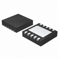
IC ADC 18BIT 3.75SPS 2CH 10-DFN
Manufacturer
Microchip Technology
Datasheet
1.MCP3422A0-EMC.pdf
(58 pages)
Specifications of MCP3423-E/MF
Data Interface
I²C, Serial
Number Of Bits
18
Sampling Rate (per Second)
3.75
Number Of Converters
1
Voltage Supply Source
Single Supply
Operating Temperature
-40°C ~ 125°C
Mounting Type
Surface Mount
Package / Case
10-DFN
Resolution (bits)
18bit
Sampling Rate
3.75SPS
Input Channel Type
Differential
Supply Voltage Range - Analog
2.7V To 5.5V
Supply Current
145µA
Digital Ic Case Style
DFN
Lead Free Status / RoHS Status
Lead free / RoHS Compliant
For Use With
MCP3423EV - BOARD EVAL 18BIT 2CH ADC MCP3423
Lead Free Status / RoHS Status
Lead free / RoHS Compliant, Lead free / RoHS Compliant


MCP3422/3/4
FIGURE 3-1:
3.3
SCL is the serial clock pin of the I
device act only as a slave and the SCL pin accepts
only external serial clocks. The input data from the
Master device is shifted into the SDA pin on the rising
edges of the SCL clock and output from the slave
device occurs at the falling edges of the SCL clock.
The SCL pin is an open-drain N-channel driver.
Therefore, it needs a pull-up resistor from the V
to the SCL pin. Refer to Section 5.3 “I
munications” for more details of I
communication.
DS22088C-page 12
Serial Clock Pin (SCL)
V
L
EGEND
R
SS
C
CHn
R
PIN
V
SS
V
T
CHn
Equivalent Analog Input Circuit.
=
=
=
=
=
Signal Source
Source Impedance
Analog Input Pin
Input Pin Capacitance
Threshold Voltage
4 pF
C
2
PIN
2
C Serial Interface
C interface. The
2
C Serial Com-
D
D
1
2
V
DD
DD
V
V
T
T
line
= 0.6V
= 0.6V
I
V
LEAKEAGE
C
SS
SAMPLE
D
1
, D
3.4
SDA is the serial data pin of the I
pin is used for input and output data. In read mode, the
conversion result is read from the SDA pin (output). In
write mode, the device configuration bits are written
(input) though the SDA pin. The SDA pin is an open-
drain N-channel driver. Therefore, it needs a pull-up
resistor from the V
start and stop conditions, the data on the SDA pin must
be stable during the high period of the clock. The high
or low state of the SDA pin can only change when the
clock signal on the SCL pin is low. Refer to Section 5.3
“I
Serial Interface communication.
Typical range of the pull-up resistor value for SCL and
SDA is from 5 kΩ to 10 kΩ for standard (100 kHz) and
fast (400 kHz) modes, and less than 1 kΩ for high
speed mode (3.4 MHz).
3.5
There is an internal electrical connection between the
Exposed Thermal Pad (EP) and the V
be connected to the same potential on the Printed
Circuit Board (PCB).
SS
R
I
(~ ±1 nA)
2
LEAKAGE
S
2
C Serial Communications” for more details of I
=
=
=
=
=
Exposed Thermal Pad (EP)
Serial Data Pin (SDA)
Leakage Current at Analog Pin
Sampling Switch
Sampling Switch Resistor
Sample Capacitance
ESD Protection Diode
SS
DD
Sampling
Switch
line to the SDA pin. Except for
© 2009 Microchip Technology Inc.
R
S
2
C interface. The SDA
C
(3.2 pF)
SS
SAMPLE
pin; they must
2
C
Related parts for MCP3423-E/MF
Image
Part Number
Description
Manufacturer
Datasheet
Request
R

Part Number:
Description:
IC ADC 18BIT 3.75SPS 2CH 10-MSOP
Manufacturer:
Microchip Technology
Datasheet:

Part Number:
Description:
Manufacturer:
Microchip Technology Inc.
Datasheet:
Part Number:
Description:
Manufacturer:
Microchip Technology Inc.
Datasheet:
Part Number:
Description:
Manufacturer:
Microchip Technology Inc.
Datasheet:
Part Number:
Description:
Manufacturer:
Microchip Technology Inc.
Datasheet:
Part Number:
Description:
Manufacturer:
Microchip Technology Inc.
Datasheet:
Part Number:
Description:
Manufacturer:
Microchip Technology Inc.
Datasheet:
Part Number:
Description:
Manufacturer:
Microchip Technology Inc.
Datasheet:
Part Number:
Description:
Manufacturer:
Microchip Technology Inc.
Datasheet: