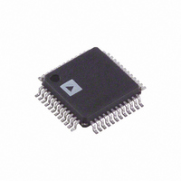
AD9875BST Analog Devices Inc, AD9875BST Datasheet - Page 22

AD9875BST
Manufacturer Part Number
AD9875BST
Description
IC 10BIT MODEM MXFE 48-LQFP
Manufacturer
Analog Devices Inc
Datasheet
1.AD9875BST.pdf
(28 pages)
Specifications of AD9875BST
Rohs Status
RoHS non-compliant
Number Of Bits
10
Number Of Channels
1
Power (watts)
950mW
Voltage - Supply, Analog
3V
Voltage - Supply, Digital
3.3V
Package / Case
48-LQFP
Main Category
Single Chip
Sub-category
Converter
Power Supply Type
Analog/Digital
Operating Supply Voltage (typ)
3.3V
Package Type
LQFP
Operating Supply Voltage (min)
3V
Operating Supply Voltage (max)
3.6V
Supply Current
262mA
Operating Temp Range
-40C to 85C
Operating Temperature Classification
Industrial
Pin Count
48
Mounting
Surface Mount
Lead Free Status / RoHS Status
Not Compliant
Available stocks
Company
Part Number
Manufacturer
Quantity
Price
Company:
Part Number:
AD9875BST
Manufacturer:
ADI
Quantity:
315
AD9875
Bit 2: Wideband Rx LPF
This bit selects the nominal cutoff frequency of the 4-pole LPF.
Setting this bit high selects a nominal cutoff frequency of 28.8 MHz.
When the wideband filter is selected, the Rx path gain is limited
to 30 dB.
Bit 3: Fast ADC Sampling
Setting this bit increases the quiescent current in the SVGA
block. This may provide some performance improvement
when the ADC sampling frequency is greater than 50 MSPS
(in 6-bit mode).
Bit 4: Rx Digital HPF Bypass
Setting this bit high bypasses the 1-pole digital HPF that follows
the ADC. The digital filter must be bypassed for ADC sampling
above 50 MSPS.
Bit 5: Rx Path DC Offset Correction
Writing a One to this bit triggers an immediate receive path
offset correction and reads back zero after the completion of the
offset correction.
Bit 6: Rx LPF Tuning Update In Progress
This bit indicates when receive filter calibration is in progress.
The duration of a receive filter calibration is about 500 ms.
Writing to this bit has no effect.
Bit 7: Rx LPF Tuning Update Disable
Setting this bit high disables the automatic background receive
filter calibration. The AD9875 automatically calibrates the
receive filter on reset and every few (~2) seconds thereafter to
compensate for process and temperature variation, power supply
and long term drift. Programming a one to this bit disables this
function. Programming a zero triggers an immediate first cali-
bration and enables the periodic update.
REGISTER 5—RECEIVE FILTER TUNING TARGET
This register sets the filter tuning target as a function of f
See Register 4 description.
REGISTER 6—Rx PATH GAIN ADJUST
The AD9875 uses a combination of a continuous time PGA
(CPGA) and a switched capacitor PGA (SPGA) for a gain range
of –6 to 36 dB with a resolution of 2 dB. The Rx path gain can
be programmed over the serial interface by writing to the Rx
Path Gain Adjust register or directly using the GAIN and MSB
aligned Tx[5:1] bits. The register default value is 0 × 00 for
lowest gain setting (–6 dB). The register always reads back the
actual gain setting irrespective of which of the two programming
modes were used.
Table V describes the gains and how they are achieved as a
function of the Rx Path adjust bits.
Bit 5: PGA Gain Set through Register
Setting this bit high will result in the Rx Path Gain being set by
writing to the PGA Gain Control register. Default is zero which
selects writing the gain through the Tx[5:1] pins in conjunction
with the gain pin.
OSCIN
.
–22–
Rx Path
Gain [4:0]
0 × 00
0 × 01
0 × 02
0 × 03
0 × 04
0 × 05
0 × 06
0 × 07
0 × 08
0 × 09
0 × 0A
0 × 0B
0 × 0C
0 × 0D
0 × 0E
0 × 0F
0 × 10
0 × 11
0 × 12*
0 × 13*
0 × 14*
0 × 15*
*When the Wideband Rx Filter bit is set high, the Rx Path Gain is limited to
REGISTER 7—TRANSMIT PATH SETTINGS
The AD9875 transmit path has a programmable interpolation
filter that precedes the transmit DAC. The interpolation filter
can be programmed to operate in seven different modes. Also,
the digital interface can be programmed to operate in several
different modes. These modes are described below.
Bit 0: Transmit Port Demultiplexer Bypass
Setting Bit 0 high bypasses the input data demultiplexer. In this
mode, consecutive nibbles on the TxDATA(5:0) pins are treated
as individual words to be sent through the Tx path. This creates
a six bit data path. The state of TxSYNC is ignored in this mode.
Bit 1: Transmit Port Width
If Bit 1 is set high, the Tx port will operate such that the most
significant nibble and the least significant nibble are each five
bits wide. The default mode is six bits for the most significant
nibble and four bit for the least significant nibble. The data is
always aligned to the MSB pin Tx[5]. Enabling this pin on the
AD9875 allows for a five pin versus the default six pin interface.
Bit 2: Transmit Port Least Significant Nibble First
Setting Bit 2 high reconfigures the AD9875 for a transmit
mode that expects least significant nibble before the most
significant nibble.
30 dB. The first of the two values in the chart refers to this mode. The second
number refers to the mode when the lower Rx LPF cutoff frequency is chosen,
or the Rx LPF filter is bypassed.
Table V. PGA Programming Map
Rx Path
Gain
–6
–4
–2
0
2
4
6
8
10
12
14
16
18
20
22
24
26
28
30/30
30/32
30/34
30/36
CPGA
Gain
–6
–6
–6
–6
–6
–6
0
0
0
6
6
6
12
12
12
18
18
18
18/24
18/24
18/24
18/24
SPGA
Gain
0
2
4
6
8
10
6
8
10
6
8
10
6
8
10
6
8
10
12/6
12/8
12/10
12/12
REV. A


