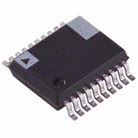
AD73311LARS Analog Devices Inc, AD73311LARS Datasheet - Page 36

AD73311LARS
Manufacturer Part Number
AD73311LARS
Description
IC ANALOG FRONT END 20-SSOP
Manufacturer
Analog Devices Inc
Datasheet
1.AD73311LAR.pdf
(36 pages)
Specifications of AD73311LARS
Rohs Status
RoHS non-compliant
Number Of Bits
16
Number Of Channels
2
Power (watts)
50mW
Voltage - Supply, Analog
3V
Voltage - Supply, Digital
3V
Package / Case
20-SSOP
Available stocks
Company
Part Number
Manufacturer
Quantity
Price
Company:
Part Number:
AD73311LARS
Manufacturer:
AD
Quantity:
12
Part Number:
AD73311LARS
Manufacturer:
ADI/亚德诺
Quantity:
20 000
Company:
Part Number:
AD73311LARS/AD73311
Manufacturer:
LITEON
Quantity:
10 000
Company:
Part Number:
AD73311LARSREEL
Manufacturer:
STM
Quantity:
6 706
Company:
Part Number:
AD73311LARSZ
Manufacturer:
MIC
Quantity:
6 222
Part Number:
AD73311LARSZ
Manufacturer:
ADI/亚德诺
Quantity:
20 000
Part Number:
AD73311LARSZ-REEL
Manufacturer:
ADI/亚德诺
Quantity:
20 000
AD73311L
APPENDIX E
DAC Timing Control Example
The AD73311’s DAC is loaded from the DAC register contents
just before the ADC register contents are loaded to the serial
register (SDOFS going high). This default DAC load position
can be advanced in time to occur earlier with respect to the SDOFS
going high. Figure 39 shows an example of the ADC unload and
DAC load sequence. At time t
that a new ADC word is ready. Following the SDOFS pulse,
16 bits of ADC data are clocked out on SDO in the subsequent
16 SCLK cycles finishing at time t
will have received the 16-bit word. The DSP may process this
information and generate a DAC word to be sent to the AD73311.
Time t
DAC word to the AD73311. This sequence ends at time t
where the DAC register will be updated from the 16 bits in the
AD73311’s serial register. However, the DAC will not be updated
from the DAC register until time t
certain applications. In order to reduce this delay and load the
DAC at time t
a suitable setting corresponding to the required time advance (refer
to Table VIII for details of DAC Timing Control settings).
0.078 (1.98)
0.068 (1.73)
0.008 (0.203)
0.002 (0.050)
3
marks the beginning of the sequence of sending the
20-Lead Shrink Small Outline IC (RS-20)
20
1
PIN 1
6
, the DAC advance register can be programmed with
0.0256
(0.65)
0.295 (7.50)
0.271 (6.90)
BSC
SEATING
PLANE
0.066 (1.67)
10
11
0.07 (1.78)
1
the SDOFS is raised to indicate
5
0.009 (0.229)
0.005 (0.127)
, which may not be acceptable in
2
0.0118 (0.30)
0.0040 (0.10)
where the DSP’s SPORT
20
1
8
0
PIN 1
0.022 (0.559)
0.037 (0.94)
0.5118 (13.00)
0.4961 (12.60)
0.0500
(1.27)
BSC
20-Lead Small Outline IC (R-20)
Dimensions shown in inches and (mm).
OUTLINE DIMENSIONS
0.0192 (0.49)
0.0138 (0.35)
0.1043 (2.65)
0.0926 (2.35)
4
11
10
SEATING
PLANE
FROM DAC
DAC LOAD
REGISTER
REGISTER
0.0125 (0.32)
0.0091 (0.23)
UPDATE
0.006 (0.15)
0.002 (0.05)
PIN 1
SDOFS
SDIFS
SCLK
SEATING
SDO
DAC
SDI
PLANE
SE
20-Lead Thin Shrink Small Outline IC (RU-20)
20
1
0.0256 (0.65)
t
8
0
1
0.0291 (0.74)
0.0098 (0.25)
0.260 (6.60)
0.252 (6.40)
BSC
0.0500 (1.27)
0.0157 (0.40)
WORD
ADC
t
0.0118 (0.30)
0.0075 (0.19)
2
0.0433 (1.10)
45
11
10
MAX
0.177 (4.50)
0.169 (4.30)
0.0035 (0.090)
0.0079 (0.20)
0.256 (6.50)
0.246 (6.25)
t
3
WORD
DAC
8
0
t
4
t
6
0.028 (0.70)
0.020 (0.50)
t
5


