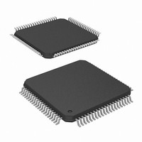
ISL98003INZ-110 Intersil, ISL98003INZ-110 Datasheet - Page 8

ISL98003INZ-110
Manufacturer Part Number
ISL98003INZ-110
Description
IC AFE 3CH 8BIT 110MHZ 80EPTQFP
Manufacturer
Intersil
Datasheet
1.ISL98003CNZ-110.pdf
(31 pages)
Specifications of ISL98003INZ-110
Number Of Bits
8
Number Of Channels
3
Power (watts)
1.1W
Voltage - Supply, Analog
1.8V, 3.3V
Voltage - Supply, Digital
1.65 V ~ 2 V
Package / Case
80-TQFP Exposed Pad, 80-eTQFP, 80-HTQFP, 80-VQFP
Lead Free Status / RoHS Status
Lead free / RoHS Compliant
Available stocks
Company
Part Number
Manufacturer
Quantity
Price
Company:
Part Number:
ISL98003INZ-110
Manufacturer:
GE
Quantity:
340
Pin Descriptions
DTEST1, 2, 3, 4, 5
CLOCKINV
HSYNC
VSYNC
EXTCLK
VADC
TEST
XCLK
DATACLK
DATACLK
CLAMP
XTAL
VPLL
VPLL
SYMBOL
RESET
XTAL
HS
FIELD
R[7:0]
G[7:0]
B[7:0]
V
V
V
V
GND
SCL
SDA
INT
DE
A3.3
A1.8
D3.3
D1.8
OUT
OUT
A3.3
D1.8
OUT
OUT
D1.8
IN
OUT
OUT
IN
IN
IN
For production use only. Tie to GND.
Digital 3.3V input.When this input is high and external CLAMP is selected, connects the selected channels inputs to the
clamp DAC.
Digital 3.3V input. When high, changes the pixel sampling phase by 180°. Toggle at frame rate during VSYNC to allow 2x
undersampling to sample odd and even pixels on sequential frames. Tie to D
3.3V digital output. A delayed version of internal COAST or CLAMP when selected.
Digital 3.3V input, active low, 70kΩ pull-up to V
pin is not necessary for normal use and may be tied directly to the V
Analog input. Connect to external 12MHz to 27MHz crystal and load capacitor (see crystal spec for recommended loading).
Typical oscillation amplitude is 1.0V
Analog output. Connect to external 12MHz to 27MHz crystal and load capacitor (see crystal spec for recommended
loading). Typical oscillation amplitude is 1.0V
3.3V digital output. Buffered crystal clock output at f
components.
Digital input, 5V tolerant, 500mV hysteresis. Serial data clock for 2-wire interface.
Bidirectional Digital I/O, open drain, 5V tolerant. Serial data I/O for 2-wire interface.
Digital 3.3V input. External clock input for AFE.
3.3V digital output. 8-bit Red channel pixel data.
3.3V digital output. 8-bit Green channel pixel data.
3.3V digital output. 8-bit Blue channel pixel data.
3.3V digital output. Data (pixel) clock output.
3.3V digital output. Inverse of DATACLK.
3.3V digital output. HSYNC output aligned with pixel data. Use this output to frame the digital output data. This output is
always purely horizontal sync (without any composite sync signals).
3.3V digital output. Buffered HSYNC (or SOG or CSYNC) output. This is typically used for measuring HSYNC period. This
output will pass composite sync signals and Macrovision signals if present on HSYNC
3.3V digital output. Buffered VSYNC output. For composite sync signals, this output will be asserted for the duration of the
disruption of the normal HSYNC pattern. This is typically used for measuring VSYNC period.
Digital output, open drain, 5V tolerant. Interrupt output indicating mode change or command execution status. Pull high
with a 4.7k resistor.
3.3V digital output. High when there is valid video data, low during horizontal and vertical blanking periods.
3.3V digital output. For interlaced video, this output will changes states to indicate whether current field is even or odd.
Polarity is determined by configuration register.
Power supply for the analog section. Connect to a 3.3V supply and bypass each pin to GND with 0.1µF.
Power supply for the analog section. Connect to a 1.8V supply and bypass each pin to GND with 0.1µF.
Power supply for the analog PLL section. Connect to a 3.3V supply and bypass to GND with 0.1µF.
Ground return connected to exposed pad.
Power supply for all digital I/Os. Connect to a 3.3V supply and bypass each pin to GND with 0.1µF.
Power supply for digital core logic. Connect to a 1.8V supply and bypass each pin to GND with 0.1µF.
Power supply for the digital ADC section. Connect to a 1.8V supply and bypass to GND with 0.1µF.
Power supply for the digital PLL section. Connect to a 1.8V supply and bypass to GND with 0.1µF.
(Continued)
8
P-P
centered around 0.5V.
ISL98003
P-P
D
. Take low for at least 1µs and then high again to reset the ISL98003. This
centered around 0.5V.
XTAL
DESCRIPTION
or f
XTAL
/2. May be used as system clock for other system
D
supply.
GND
if unused.
IN
or SOG
IN
.
September 12, 2008
FN6760.0


