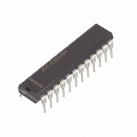
DS1742-70 Maxim Integrated Products, DS1742-70 Datasheet

DS1742-70
Specifications of DS1742-70
Available stocks
Related parts for DS1742-70
DS1742-70 Summary of contents
Page 1
... Disconnected to Retain Freshness until Power is Applied for the First Time Standard JEDEC Bytewide Static RAM Pinout Quartz Accuracy ±1 Minute a Month at +25°C, Factory Calibrated UL Recognized ORDERING INFORMATION PART VOLTAGE (V) DS1742-70 DS1742-70+ DS1742-100 DS1742-100+ DS1742-100IND DS1742-100IND+ DS1742W-120 DS1742W-120+ DS1742W-150 DS1742W-150+ DS1742P-100+ +Denotes a lead-free/RoHS-compliant device. ...
Page 2
... The RTC clock registers are double-buffered to avoid access of incorrect data that can occur during clock update cycles. The double-buffered system also prevents time loss as the timekeeping countdown continues unabated by access to time register data. The DS1742 also contains its own power-fail circuitry, which deselects the device when the V loss of data from unpredictable system operation brought on by low V cycles are avoided ...
Page 3
... CLOCK OPERATIONS—READING THE CLOCK While the double-buffered register structure reduces the chance of reading incorrect data, internal updates to the DS1742 clock registers should be halted before clock data is read to prevent reading of data in transition. However, halting the internal clock register updating process does not affect clock accuracy. ...
Page 4
... As shown in Table 2, bit 7 of the century register is the write bit. Setting the write bit like the read bit, halts updates to the DS1742 registers. The user can then load them with the correct day, date and time data in 24-hour BCD format. Resetting the write bit then transfers those values to the actual clock counters and allows normal operation to resume ...
Page 5
... AA inputs are changed while CE time (t ) but will then go indeterminate until the next address access. OH WRITING DATA TO RAM OR CLOCK The DS1742 is in the write mode whenever referenced to the latter occurring transition of the cycle. or must return inactive for a minimum write cycle. Data in must be valid t typical application, the signal will be high during a write cycle ...
Page 6
... The DS1742 has a lithium power source that is designed to provide energy for clock activity, and clock and RAM data retention when the V is sufficient to power the DS1742 continuously for the life of the equipment in which it is installed. For specification purposes, the life expectancy is 10 years at 25°C with the internal clock oscillator running in the absence of V power ...
Page 7
ABSOLUTE MAXIMUM RATINGS Voltage Range on Any Pin Relative to Ground……………………………………………..-0.3V to +6.0V Operating Temperature Range……………………………………………...0°C to +70°C (noncondensing) Storage Temperature Range………………………………………………………………...-40°C to +85°C Soldering Temperature (EDIP, leads)..………………………………..+260°C for 10 seconds (See Note 7) This is a stress rating only ...
Page 8
DC ELECTRICAL CHARACTERISTICS = 3.3V ±10%, Over the operating range PARAMETER Active Supply Current TTL Standby Current ( = V CE CMOS Standby Current ³ 0.2V Input Leakage Current (any input) Output Leakage ...
Page 9
AC CHARACTERISTICS—READ CYCLE (3.3V) = 3.3V ±10%, Over the operating range PARAMETER Read Cycle Time Address Access Time to DQ Low-Z CE Access Time CE Data Off time Low-Z OE Access Time OE Data Off ...
Page 10
AC CHARACTERISTICS—WRITE CYCLE (5V) = 5.0V ±10%, Over the operating range PARAMETER Write Cycle Time Address Access Time Pulse Width WE Pulse Width CE Data Setup Time Data Hold time Address Hold Time Data Off Time WE Write ...
Page 11
WRITE CYCLE TIMING DIAGRAM—WRITE-ENABLE CONTROLLED WRITE CYCLE TIMING DIAGRAM—CHIP-ENABLE CONTROLLED ...
Page 12
POWER-UP/POWER-DOWN CHARACTERISTICS (5V) = 5.0V ±10%, Over the operating range PARAMETER Before Power-Down Fall Time PF(MAX) V Fall Time PF(MIN) V Rise ...
Page 13
POWER-UP/POWER-DOWN CHARACTERISTICS (3.3V) = 3.3V ±10%, Over the operating range PARAMETER Before Power-Down Fall Time PF(MAX) V Rise Time PF(MIN) Power-Up Recovery ...
Page 14
... Typical values are at 25°C and nominal supplies. 3) Outputs are open. 4) Battery switchover occurs at the lower of either the battery voltage Data retention time is at 25°C. 6) Each DS1742 has a built-in switch that disconnects the lithium source until V user. The expected t is defined as a cumulative time in the absence power is first applied by the user ...
Page 15
... For the latest package outline information www.maxim-ic.com/DallasPackInfo.) DS1742 24-PIN PACKAGE Maxim/Dallas Semiconductor cannot assume responsibility for use of any circuitry other than circuitry entirely embodied in a Maxim/Dallas Semiconductor product. ...


