DS12887A Maxim Integrated Products, DS12887A Datasheet - Page 9
DS12887A
Manufacturer Part Number
DS12887A
Description
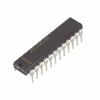
IC RTC W/RAM 128 BYTE 24-EDIP
Manufacturer
Maxim Integrated Products
Type
Clock/Calendar/NVSRAMr
Datasheet
1.DS12885Q.pdf
(22 pages)
Specifications of DS12887A
Memory Size
114B
Time Format
HH:MM:SS (12/24 hr)
Date Format
YY-MM-DD-dd
Interface
Parallel
Voltage - Supply
4.5 V ~ 5.5 V
Operating Temperature
0°C ~ 70°C
Mounting Type
Through Hole
Package / Case
24-DIP (600 mil) Module
Lead Free Status / RoHS Status
Contains lead / RoHS non-compliant
Available stocks
Company
Part Number
Manufacturer
Quantity
Price
Company:

Part Number:
DS12887A
Manufacturer:
DALLAS
Quantity:
5 380
Company:
Part Number:
DS12887A
Manufacturer:
DALLAS
Quantity:
5 380
Company:
Part Number:
DS12887A
Manufacturer:
DALLAS
Quantity:
114
Company:
Part Number:
DS12887A
Manufacturer:
DALLAS
Quantity:
26
Company:
Part Number:
DS12887A
Manufacturer:
DALLAS
Quantity:
5 510
Part Number:
DS12887A+
Manufacturer:
MAXIM/美信
Quantity:
20 000


PDIP
SO,
22
17
18
16, 20,
21, 22
EDIP
2, 3,
17
18
PIN
13, 18,
PLCC
1, 11,
26
21
22
4, 6, 10,
15, 20,
23, 25,
27, 32
TQFP
18
19
RESET
NAME
N.C.
DS
_____________________________________________________________________
No Connection. This pin should remain unconnected. Pin 21 is RCLR for the
DS12887A/DS12C887A. On the EDIP, these pins are missing by design.
D ata S tr ob e or Read Inp ut. The D S p i n has tw o m od es of op er ati on d ep end i ng on
the l evel of the M O T p i n. W hen the M O T p i n i s connected to V
ti m i ng i s sel ected . In thi s m od e, D S i s a p osi ti ve p ul se d ur i ng the l atter p or ti on of the
b us cycl e and i s cal l ed d ata str ob e. D ur i ng r ead cycl es, D S si g ni fi es the ti m e that the
device i s to d r i ve the b i d i r ecti onal b us. In w r i te cycl es, the tr ai l i ng ed g e of D S causes
the device to l atch the w r i tten d ata. W hen the M O T p i n i s connected to GN D , Intel
b us ti m i ng i s sel ected . D S i d enti fi es the ti m e p er i od w hen the device d r i ves the b us
w i th r ead d ata. In thi s m od e, the D S p i n op er ates i n a si m i l ar fashi on as the outp ut-
enab l e ( O E ) si g nal on a g ener i c RAM .
Active-Low Reset Input. The RESET pin has no effect on the clock, calendar, or
RAM. On power-up, the RESET pin can be held low for a time to allow the power
supply to stabilize. The amount of time that RESET is held low is dependent on the
application. However, if RESET is used on power-up, the time RESET is low should
exceed 200ms to ensure that the internal timer that controls the device on power-
up has timed out. When RESET is low and V
In a typical application, RESET can be connected to V
the device to go in and out of power fail without affecting any of the control
registers.
A. Periodic interrupt-enable (PIE) bit is cleared to 0.
B. Alarm interrupt-enable (AIE) bit is cleared to 0.
C. Update-ended interrupt-enable (UIE) bit is cleared to 0.
D. Periodic-interrupt flag (PF) bit is cleared to 0.
E. Alarm-interrupt flag (AF) bit is cleared to 0.
F. Update-ended interrupt flag (UF) bit is cleared to 0.
G. Interrupt-request status flag (IRQF) bit is cleared to 0.
H. IRQ pin is in the high-impedance state.
I. The device is not accessible until RESET is returned high.
J. Square-wave output-enable (SQWE) bit is cleared to 0.
Pin Description (continued)
Real-Time Clocks
FUNCTION
CC
is above V
CC
. This connection allows
PF
C C
, the following occurs:
, M otor ol a b us
9
Related parts for DS12887A
Image
Part Number
Description
Manufacturer
Datasheet
Request
R

Part Number:
Description:
MAX7528KCWPMaxim Integrated Products [CMOS Dual 8-Bit Buffered Multiplying DACs]
Manufacturer:
Maxim Integrated Products
Datasheet:
Part Number:
Description:
Single +5V, fully integrated, 1.25Gbps laser diode driver.
Manufacturer:
Maxim Integrated Products
Datasheet:
Part Number:
Description:
Single +5V, fully integrated, 155Mbps laser diode driver.
Manufacturer:
Maxim Integrated Products
Datasheet:
Part Number:
Description:
VRD11/VRD10, K8 Rev F 2/3/4-Phase PWM Controllers with Integrated Dual MOSFET Drivers
Manufacturer:
Maxim Integrated Products
Datasheet:
Part Number:
Description:
Highly Integrated Level 2 SMBus Battery Chargers
Manufacturer:
Maxim Integrated Products
Datasheet:
Part Number:
Description:
Current Monitor and Accumulator with Integrated Sense Resistor; ; Temperature Range: -40°C to +85°C
Manufacturer:
Maxim Integrated Products
Part Number:
Description:
TSSOP 14/A�/RS-485 Transceivers with Integrated 100O/120O Termination Resis
Manufacturer:
Maxim Integrated Products
Part Number:
Description:
TSSOP 14/A�/RS-485 Transceivers with Integrated 100O/120O Termination Resis
Manufacturer:
Maxim Integrated Products
Part Number:
Description:
QFN 16/A�/AC-DC and DC-DC Peak-Current-Mode Converters with Integrated Step
Manufacturer:
Maxim Integrated Products
Part Number:
Description:
TDFN/A/65V, 1A, 600KHZ, SYNCHRONOUS STEP-DOWN REGULATOR WITH INTEGRATED SWI
Manufacturer:
Maxim Integrated Products
Part Number:
Description:
Integrated Temperature Controller f
Manufacturer:
Maxim Integrated Products
Part Number:
Description:
SOT23-6/I�/45MHz to 650MHz, Integrated IF VCOs with Differential Output
Manufacturer:
Maxim Integrated Products
Part Number:
Description:
SOT23-6/I�/45MHz to 650MHz, Integrated IF VCOs with Differential Output
Manufacturer:
Maxim Integrated Products
Part Number:
Description:
EVALUATION KIT/2.4GHZ TO 2.5GHZ 802.11G/B RF TRANSCEIVER WITH INTEGRATED PA
Manufacturer:
Maxim Integrated Products
Part Number:
Description:
QFN/E/DUAL PCIE/SATA HIGH SPEED SWITCH WITH INTEGRATED BIAS RESISTOR
Manufacturer:
Maxim Integrated Products
Datasheet: