DS1747-70IND Maxim Integrated Products, DS1747-70IND Datasheet
DS1747-70IND
Specifications of DS1747-70IND
Available stocks


Related parts for DS1747-70IND


DS1747-70IND Summary of contents
Page 1
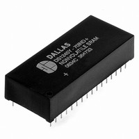
... Maxim 2 DS1747 A14 A17 A12 4 29 A13 A11 A10 DQ7 DQ0 DQ6 14 19 DQ1 DQ5 DQ2 15 18 DQ4 17 GND 16 DQ3 Encapsulated DIP (512k Maxim 33 2 DS1747P GND BAT PowerCap Module Board (Uses DS9034PCX PowerCap) A18 A17 A14 A13 A12 A11 A10 ...
Page 2
... Pin Configuration) (See Pin — Configuration) DS1747/DS1747P Y2K-Compliant, Nonvolatile Timekeeping RAMs NAME FUNCTION A18 A16 A14 A12 Address Input A10 A11 A9 A8 A13 A17 A15 DQ0 DQ1 DQ2 DQ3 Data Input/Output DQ4 DQ5 DQ6 DQ7 GND Ground ...
Page 3
... PIN-PACKAGE TOP MARK 32 EDIP (0.740a) DS1747-70+ 32 EDIP (0.740a) DS1747-70IND+ 34 PowerCap* DS1747P+70 34 PowerCap* DS1747P+70 IND 32 EDIP (0.740a) DS1747W-120+ 32 EDIP (0.740a) DS1747W-120IND+ 34 PowerCap* DS1747WP+120 34 PowerCap* DS1747WP+120 IND supply out-of- CC † ...
Page 4
... CLOCK OPERATIONS—READING THE CLOCK While the double-buffered register structure reduces the chance of reading incorrect data, internal updates to the DS1747 clock registers should be halted before clock data is read to prevent reading of data in transition. However, halting the internal clock register updating process does not affect clock accuracy ...
Page 5
... As shown in Table 2, bit 7 of the century register is the write bit. Setting the write bit to a one, like the read bit, halts updates to the DS1747 registers. The user can then load them with the correct day, date and time data in 24-hour format. Resetting the write bit to a zero then transfers those values to the actual clock counters and allows normal operation to resume ...
Page 6
... OH WRITING DATA TO RAM OR CLOCK The DS1747 is in the write mode whenever WE, and CE are in their active state. The start of a write is referenced to the latter occurring transition CE. The addresses must be held valid throughout the cycle must return inactive for a minimum of t write cycle ...
Page 7
... The DS1747 has a lithium power source that is designed to provide energy for clock activity, and clock and RAM data retention when the V is sufficient to power the DS1747 continuously for the life of the equipment in which it is installed. For specification purposes, the life expectancy is 10 years at +25C with the internal clock oscillator running in the absence of V power ...
Page 8
... CE 0.2V) CC Input Leakage Current (Any Input) Output Leakage Current (Any Output) Output Logic 1 Voltage (I = -1.0mA) OUT Output Logic 0 Voltage (I = +2.1mA) OUT Write Protection Voltage Battery Switchover Voltage DS1747/DS1747P Y2K-Compliant, Nonvolatile Timekeeping RAMs SYMBOL MIN TYP -0.3 IL SYMBOL ...
Page 9
... AC CHARACTERISTICS—READ CYCLE (5V) = 5.0V 10 Over the Operating Range PARAMETER Read Cycle Time Address Access Time Low Access Time CE Data Off Time Low-Z OE Access Time OE Data Off Time Output Hold from Address DS1747/DS1747P Y2K-Compliant, Nonvolatile Timekeeping RAMs SYMBOL MIN TYP Icc Icc 1 Icc ...
Page 10
... Over the Operating Range PARAMETER Read Cycle Time Address Access Time Low Access Time CE Data Off Time Low-Z OE Access Time OE Data Off Time Output Hold from Address READ CYCLE TIMING DIAGRAM DS1747/DS1747P Y2K-Compliant, Nonvolatile Timekeeping RAMs SYMBOL MIN TYP t 120 CEL t CEA ...
Page 11
... Write Cycle Time Address Setup Time WE Pulse Width CE Pulse Width CE and CE2 Pulse Width Data Setup Time Data Hold Time Data Hold Time Address Hold Time Address Hold Time WE Data Off Time Write Recovery Time DS1747/DS1747P Y2K-Compliant, Nonvolatile Timekeeping RAMs SYMBOL MIN TYP ...
Page 12
... WRITE CYCLE TIMING DIAGRAM, WRITE-ENABLE CONTROLLED WRITE CYCLE TIMING DIAGRAM, CHIP-ENABLE CONTROLLED DS1747/DS1747P Y2K-Compliant, Nonvolatile Timekeeping RAMs ...
Page 13
... Fall Time PF(MAX) V PF(MIN) V Fall Time PF(MIN Rise Time PF(MIN MAX) Power-Up Recover Time VPF to RST High (PowerCap Only) Expected Data-Retention Time (Oscillator ON) POWER-UP/DOWN TIMING (5V DEVICE) DS1747/DS1747P Y2K-Compliant, Nonvolatile Timekeeping RAMs SYMBOL MIN TYP 300 REC MAX UNITS NOTES s s ...
Page 14
... PF(MAX) Power-Up Recover Time V to RST High (PowerCap PF Only) Expected Data-Retention Time (Oscillator ON) POWER-UP/DOWN WAVEFORM TIMING (3.3V DEVICE) CAPACITANCE (T = +25°C) A PARAMETER Capacitance on All Input Pins Capacitance on All Output Pins DS1747/DS1747P Y2K-Compliant, Nonvolatile Timekeeping RAMs SYMBOL MIN TYP 300 REC t 10 ...
Page 15
... Battery switchover occurs at the lower of either the battery terminal voltage Data-retention time is at +25C. 6) Each DS1747 has a built-in switch that disconnects the lithium source until the user first applies V The expected t is defined for DIP modules and assembled PowerCap modules as accumulative time ...
Page 16
... Maxim cannot assume responsibility for use of any circuitry other than circuitry entirely embodied in a Maxim product. No circuit patent licenses are implied. Maxim reserves the right to change the circuitry and specifications without notice at any time 2010 Maxim Integrated Products DS1747/DS1747P Y2K-Compliant, Nonvolatile Timekeeping RAMs DESCRIPTION Maxim and the Dallas logo are registered trademarks of Maxim Integrated Products. ...