DS1340C-18# Maxim Integrated Products, DS1340C-18# Datasheet - Page 6
DS1340C-18#
Manufacturer Part Number
DS1340C-18#
Description
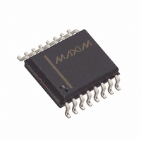
IC RTC I2C W/CHARGER 16-SOIC
Manufacturer
Maxim Integrated Products
Type
Clock/Calendar/Trickle-Chargerr
Datasheet
1.DS1340U-33.pdf
(16 pages)
Specifications of DS1340C-18#
Time Format
HH:MM:SS (24 hr)
Date Format
YY-MM-DD-dd
Interface
I²C, 2-Wire Serial
Voltage - Supply
1.71 V ~ 1.89 V
Operating Temperature
-40°C ~ 85°C
Mounting Type
Surface Mount
Package / Case
16-SOIC (0.300", 7.5mm Width)
Lead Free Status / RoHS Status
Lead free / RoHS Compliant
Memory Size
-


I
The DS1340 is a low-power clock/calendar with a trickle
charger. Address and data are transferred serially
through a I
vides seconds, minutes, hours, day, date, month, and
year information. The date at the end of the month is
automatically adjusted for months with fewer than 31
days, including corrections for leap year. The DS1340
has a built-in power-sense circuit that detects power fail-
ures and automatically switches to the backup supply.
The power-control function is provided by a precise,
temperature-compensated voltage reference and a
comparator circuit that monitors the V
device is fully accessible and data can be written and
read when V
falls below V
6
2
—
8
1
2
3
4
5
6
7
8
PIN
C RTC with Trickle Charger
_____________________________________________________________________
4–13
16
14
15
16
—
—
1
2
3
2
C bidirectional bus. The clock/calendar pro-
CC
PF
V
FT/OUT
NAME
BACKUP
GND
, the internal clock registers are blocked
SDA
SCL
N.C.
V
is greater than V
X1
X2
CC
Detailed Description
Connections for a Standard 32.768kHz Quartz Crystal. The internal oscillator circuitry is designed for
operation with a crystal having a specified load capacitance (C
and can optionally be connected to an external 32.768kHz oscillator. The output of the internal oscillator,
X2, is left unconnected if an external oscillator is connected to X1.
Connection for a Secondary Power Supply. For the 1.8V and 3V devices, V
1.3V and 3.7V for proper operation. Diodes placed in series between the supply and the input pin may
result in improper operation. V
This pin can be connected to a primary cell such as a lithium coin cell. Additionally, this pin can be
connected to a r echar g eab l e cel l or a sup er cap w hen used w i th the tr i ckl e- char g e featur e. U L r ecog ni zed to
ensure against reverse charging when used with a lithium battery (www.maxim-ic.com/qa/info/ul).
Ground
Serial Data Input/Output. SDA is the data input/output for the I
drain and requires an external pullup resistor.
Serial Clock Input. SCL is the clock input for the I
on the serial interface.
Frequency Test/Output. This pin is used to output either a 512Hz signal or the value of the OUT bit. When
the FT bit is logic 1, the FT/OUT pin toggles at a 512Hz rate. When the FT bit is logic 0, the FT/OUT pin
reflects the value of the OUT bit. This open-drain pin requires an external pullup resistor, and operates
with either V
V
P r i m ar y P ow er S up p l y. W hen vol tag e i s ap p l i ed w i thi n nor m al l i m i ts, the d evi ce i s ful l y accessi b l e and d ata
can b e w r i tten and r ead . W hen a b ackup sup p l y i s connected to the d evi ce and V
and w r i tes ar e i nhi b i ted . H ow ever , the ti m ekeep i ng functi on conti nues unaffected b y the l ow er i np ut
vol tag e.
No Connection. Must be connected to ground.
CC
. If not used, this pin can be left unconnected.
PF
Power Control
CC
. However, when V
or V
BACKUP
CC
level. The
applied. The pullup voltage can be up to 5.5V, regardless of the voltage on
BACKUP
CC
can be as high as 5.5V on the 3.3V device.
from any access. If V
device power is switched from V
V
the device power is switched from V
Table 1. Power Control
CC
SUPPLY CONDITION
FUNCTION
2
drops below V
V
V
V
V
C interface and is used to synchronize data movement
CC
CC
CC
CC
V
V
V
V
CC
CC
CC
CC
< V
> V
< V
> V
< V
< V
> V
> V
BACKUP
BACKUP
BACKUP
BACKUP
PF
PF
PF
PF
2
,
,
,
,
C serial interface. The SDA pin is open
L
) of 12.5pF. X1 is the input to the oscillator
PF
. If V
PF
READ/WRITE
BACKUP
PF
is less than V
ACCESS
Yes
Yes
is greater than V
No
No
Pin Description
C C
CC
must be held between
i s b el ow V
to V
CC
BACKUP
BACKUP
POWERED
to V
T P
, r ead s
V
V
V
V
BY
BACKUP
BAT
BACKUP
CC
CC
CC
when
, the
,
Related parts for DS1340C-18#
Image
Part Number
Description
Manufacturer
Datasheet
Request
R

Part Number:
Description:
IC RTC I2C W/CHARGER 16-SOIC
Manufacturer:
Maxim Integrated Products
Datasheet:
Part Number:
Description:
IC RTC I2C W/CHARGER 16-SOIC
Manufacturer:
Maxim Integrated Products
Datasheet:
Part Number:
Description:
IC RTC I2C W/CHARGER 16-SOIC
Manufacturer:
Maxim Integrated Products
Datasheet:

Part Number:
Description:
Real Time Clock I2C-Compatible RTC w ith Trickle Charger
Manufacturer:
Maxim Integrated Products
Datasheet:
Part Number:
Description:
Real Time Clock I2C-Compatible RTC w ith Trickle Charger
Manufacturer:
Maxim Integrated Products
Datasheet:
Part Number:
Description:
Real Time Clock
Manufacturer:
Maxim Integrated Products
Datasheet:

Part Number:
Description:
I2C RTC with Trickle Charger
Manufacturer:
MAXIM [Maxim Integrated Products]
Datasheet:
Part Number:
Description:
Ds1340, Ds1340c I?c Rtc With Trickle Charger
Manufacturer:
Maxim Integrated Products, Inc.
Datasheet:
Part Number:
Description:
Ds13 D-sub Dual Port Type
Manufacturer:
Megastar Electronics Inc.
Datasheet:
Part Number:
Description:
DS13 Series High Performance Solid State Relays For Loads Up To 2A@60Vdc
Manufacturer:
MACOM [Tyco Electronics]
Datasheet:

Part Number:
Description:
Solid State Relays HIGH FREQUENCY RELAY
Manufacturer:
Tyco Electronics

Part Number:
Description:
DS13-1002 = DS13 SOLID STATE D
Manufacturer:
TE Connectivity
Datasheet:
Part Number:
Description:
MAX7528KCWPMaxim Integrated Products [CMOS Dual 8-Bit Buffered Multiplying DACs]
Manufacturer:
Maxim Integrated Products
Datasheet: