DS1305 Maxim Integrated Products, DS1305 Datasheet
DS1305
Specifications of DS1305
Available stocks


Related parts for DS1305

DS1305 Summary of contents
Page 1
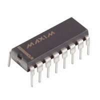
... TOP VIEW CC2 BAT DS1305 N. N. INT0 INT1 9 12 GND 10 11 TSSOP (4.4mm CC2 BAT DS1305 N. INT0 6 11 INT1 7 10 GND 8 9 DIP (300 mils) DS1305 V CC1 N. CCIF SD0 SDI SCLK N.C. CE SERMODE V CC1 PF V CCIF SDO SDI SCLK CE SERMODE ...
Page 2
... The clock operates in either the 24-hour or 12-hour format with AM/PM indicator. In addition, 96 bytes of NV RAM are provided for data storage. The DS1305 will maintain the time and date, provided the oscillator is enabled, as long as at least one supply valid level. ...
Page 3
... Active-Low Interrupt 1 Output. The INT1 pin is an active-low output of the DS1305 that can be used as an interrupt input to a processor. The INT1 pin can be programmed to be asserted by Alarm 1 only. The INT1 pin remains low as long as the status bit causing the interrupt is present and the corresponding interrupt enable bit is set ...
Page 4
... Active-Low Power-Fail Output. The PF pin is used to indicate loss of the primary power supply (V ). When V CC1 the PF pin is driven low. Primary Power Supply. DC power is provided to the device on this pin. OSCILLATOR AND COUNTDOWN CHAIN FUNCTION pin allows the DS1305 to drive CCIF is less than less than V CC1 CC2 1Hz , BAT ...
Page 5
RECOMMENDED LAYOUT FOR CRYSTAL Local ground plane (Layer 2) crystal CLOCK ACCURACY The accuracy of the clock is dependent upon the accuracy of the crystal and the accuracy of the match between the capacitive load of the oscillator circuit and ...
Page 6
... Note: Range for alarm registers does not include mask’m’ bits. The DS1305 can be run in either 12-hour or 24-hour mode. Bit 6 of the hours register is defined as the 12- or 24-hour mode select bit. When high, the 12-hour mode is selected. In the 12-hour mode, bit 5 is the AM/PM bit with logic high being PM ...
Page 7
... Oscillator) – This bit when set to logic 0 starts the oscillator. When this bit is set to a EOSC logic 1, the oscillator is stopped and the DS1305 is placed into a low-power standby mode with a current drain of less than 100nA when power is supplied by V will be set to a logic 1. ...
Page 8
... To prevent accidental enabling, only a pattern of 1010 enables the trickle charger. All other patterns disable the trickle charger. On the initial application of power, the DS1305 powers up with the trickle charger disabled. The diode select (DS) bits (bits 2–3) select whether one diode or two diodes are connected between V resistor that is connected between V bits, as shown in Table 3 ...
Page 9
... DS1305. The DS1305 does not write-protect itself in this configuration. CC2 CC2 Configuration 3 shows the DS1305 in battery operate mode where the device is powered only by a single battery. In this case, the V CC1 Only these three configurations are allowed. Unused supply pins must be grounded. ...
Page 10
Figure 4. POWER-SUPPLY CONFIGURATIONS NOTE: DEVICE IS WRITE-PROTECTED IF V NOTE: DEVICE DOES NOT PROVIDE AUTOMATIC WRITE PROTECTION. CONFIGURATION 1: BACKUP SUPPLY IS NONRECHARGEABLE LITHIUM BATTERY < CCTP CONFIGURATION 2: BACKUP SUPPLY IS A RECHARGEABLE BATTERY OR ...
Page 11
... SCLK (serial clock). The DS1305 is the slave device in an SPI application, with the microcontroller being the master. The SDI and SDO pins are the serial data input and output pins for the DS1305, respectively. The CE input is used to initiate and terminate a data transfer. The SCLK pin is used to synchronize data movement between the master (microcontroller) and the slave (DS1305) devices ...
Page 12
... Data transfers can occur one byte at a time or in multiple-byte burst mode. After CE is driven high an address is written to the DS1305. After the address, one or more data bytes can be written or read. For a single-byte transfer, one byte is read or written and then CE is driven low. For a multiple-byte transfer, however, multiple bytes can be read or written to the DS1305 after the address has been written ...
Page 13
Figure 8. SPI MULTIPLE-BYTE BURST TRANSFER READING AND WRITING IN BURST MODE Burst mode is similar to a single-byte read or write, except that CE is kept high and additional SCLK cycles are sent until the end of the burst. ...
Page 14
INTERFACE The 3-wire interface mode operates similarly to the SPI mode. However, in 3-wire mode there is one I/O instead of separate data in and data out signals. The 3-wire interface consists of the I/O (SDI and SDO pins ...
Page 15
ABSOLUTE MAXIMUM RATINGS Voltage Range on Any Pin Relative to Ground……………………………………………..-0.5V to +7.0V Storage Temperature Range……………………………………………………………….-55°C to +125°C Soldering Temperature………………………………………….See IPC/JEDEC J-STD-020 Specification This is a stress rating only and functional operation of the device at these or any other ...
Page 16
DC ELECTRICAL CHARACTERISTICS (Over the operating range, unless otherwise specified.) PARAMETER Input Leakage Output Leakage I = 1.5mA Logic 0 OL Output I = 4.0mA -0.4mA Logic 1 OH Output I = -1.0mA OH V Active Supply ...
Page 17
AC ELECTRICAL CHARACTERISTICS (Over the operating range, unless otherwise specified.) (Figure 10 and Figure 11) PARAMETER Data to CLK Setup CLK to Data Hold CLK to Data Delay CLK Low Time CLK High Time CLK Frequency CLK Rise and ...
Page 18
Figure 10. TIMING DIAGRAM: 3-WIRE READ DATA TRANSFER SERMODE = GND * I/O IS SDI AND SDO TIED TOGETHER. Figure 11. TIMING DIAGRAM: 3-WIRE WRITE DATA TRANSFER SERMODE = GND * I/O IS SDI AND SDO TIED TOGETHER ...
Page 19
SPI AC ELECTRICAL CHARACTERISTICS (Over the operating range, unless otherwise specified.) (Figure 12 and Figure 13) PARAMETER Data to CLK Setup CLK to Data Hold CLK to Data Delay CLK Low Time CLK High Time CLK Frequency CLK Rise and ...
Page 20
Figure 12. TIMING DIAGRAM: SPI READ DATA TRANSFER SERMODE = SCLK CAN BE EITHER POLARITY, TIMING SHOWN FOR CPOL = 1. Figure 13. TIMING DIAGRAM: SPI WRITE DATA TRANSFER SERMODE = SCLK CAN BE ...
Page 21
NOTES and I are specified with CE set to a logic 0 and CC1T CC2T 2) I and I are specified with CC1A CC2A 2.0V 0V ...
Page 22
... Maxim cannot assume responsibility for use of any circuitry other than circuitry entirely embodied in a Maxim product. No circuit patent licenses are implied. Maxim reserves the right to change the circuitry and specifications without notice at any time © 2009 Maxim Integrated Products DESCRIPTION ” to Figures 6, 7, 12, and 13 Maxim is a registered trademark of Maxim Integrated Products, Inc. DS1305 PAGES CHANGED 5 12 ...