DP8573AVX/NOPB National Semiconductor, DP8573AVX/NOPB Datasheet - Page 13
DP8573AVX/NOPB
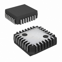
Manufacturer Part Number
DP8573AVX/NOPB
Description
IC REAL TIME CLOCK (RTC) 28-PLCC
Manufacturer
National Semiconductor
Type
Clock/Calendar/NVSRAMr
Datasheet
1.DP8573AVXNOPB.pdf
(16 pages)
Specifications of DP8573AVX/NOPB
Memory Size
32B
Time Format
HH:MM:SS:hh (12/24 hr)
Date Format
YY-MM-DD-dd
Interface
Parallel
Voltage - Supply
4.5 V ~ 5.5 V
Operating Temperature
-40°C ~ 85°C
Mounting Type
Surface Mount
Package / Case
28-PLCC
Bus Type
Parallel
Operating Supply Voltage (typ)
5V
Package Type
PLCC
Operating Supply Voltage (max)
5.5V
Operating Supply Voltage (min)
4.5V
Operating Temperature Classification
Industrial
Operating Temperature (max)
85C
Operating Temperature (min)
-40C
Pin Count
28
Mounting
Surface Mount
Lead Free Status / RoHS Status
Lead free / RoHS Compliant
Other names
*DP8573AVX
*DP8573AVX/NOPB
DP8573AVX
*DP8573AVX/NOPB
DP8573AVX
Available stocks
Company
Part Number
Manufacturer
Quantity
Price
Company:

Part Number:
DP8573AVX/NOPB
Manufacturer:
Texas Instruments
Quantity:
10 000


Main Status Register PS
Periodic Flag Register PS
Time Save Control Register PS
Real Time Mode Register PS
Output Mode Register PS
Interrupt Control Register 0 PS
Interrupt Control Register 1 PS
Control and Status Register Address Bit Map
Time Save
Power Fail
Application Hints
Suggested Initialization Procedure for DP8573A in Bat-
tery Backed Applications that use the V
1
2
3
Interrupt
MFO as
Enable
Enable
Crystal
Mode
R W
RAM
R W
RAM
RAM
Test
Enter the test mode by writing a 1 to bit D7 in the Period-
ic Flag Register
Write zero to the RAM TEST mode Register located in
page 0 address HEX 1F
Leave the test mode by writing a 0 to bit D7 in the Peri-
odic Flag Register Steps 1 2 3 guarantee that if the
test mode had been entered during power on (due to
random pulses from the system) all test mode condi-
tions are cleared Most important is that the OSC Fail
Disable bit is cleared Refer to AN-589 for more informa-
tion on test mode operation
D7
Single Supply
Osc Fail
Register
Interrupt
Enable
Select
R W
Alarm
R W
RAM
RAM
RAM
N A
D6
4
e
e
e
X RS
0
0
e
Interrupt
Interrupt
Enable
Enable
e
0
e
e
DOW
RAM
RAM
RAM
RAM
R W
1 ms
1 ms
Flag
D5
R
0
e
0
0
5
RS
RS
X ADDRESS
RS
e
e
RS
RS
RS
BB
Interrupt EN
on Back-Up
0
1
e
Interrupt
Interrupt
Enable
Enable
Month
10 ms
10 ms
Pin
e
RAM
RAM
1
RAM
e
e
R W
Flag
D4
R
0 Address
5
1
1
Address
Address
e
Address
00H
Address
Address
Start Stop
Interrupt
Interrupt
Interrupt
100 ms
100 ms
Enable
Enable
R W
Alarm
Clock
e
e
e
RAM
RAM
DOM
Flag
D3
R
13
02H
03H
5
04H
e
1
01H
e
e
4
4 1 Write a 1 to bit D3 in the Real Time Mode Register (try
03H
04H
Enter a software loop that does the following
Set a 3 second(approx) software counter The crystal
oscillator may take 1 second to start
to start the clock) Under normal operation this bit can
be set only if the oscillator is running During the soft-
ware loop RAM real time counters output configura-
tion interrupt control and timer functions may be initial-
ized
12 24 Hr
Seconds
Seconds
Interrupt
Interrupt
Interrupt
Periodic
Enable
Enable
R W
Mode
Hours
RAM
RAM
Flag
D2
R
5
1
10 Second
10 Second
Power Fail
Leap Year
Interrupt
Interrupt
Interrupt
Enable
Minute
Enable
RAM
RAM
MSB
Flag
D1
R
R
2
5
Leap Year
Interrupt
Interrupt
Interrupt
Second
Minute
Minute
Enable
Enable
Status
RAM
RAM
Flag
LSB
D0
R
R
3
5
1 Reset by
2 Set reset by
3 Reset when
4 Read Osc fail
5 Reset by
All Bits R W
All Bits R W
All Bits R W
All Bits R W
All Bits R W
writing
1 to bit
voltage at
PFAIL pin
all pending
interrupts
are removed
Write 0 Batt-
Backed Mode
Write 1 Single
Supply Mode
positive edge
of read
Related parts for DP8573AVX/NOPB
Image
Part Number
Description
Manufacturer
Datasheet
Request
R

Part Number:
Description:
IC REAL TIME CLOCK (RTC) 28-PLCC
Manufacturer:
National Semiconductor
Datasheet:

Part Number:
Description:
Clock IC
Manufacturer:
National Semiconductor
Datasheet:

Part Number:
Description:
National Semiconductor [8-Bit D/A Converter]
Manufacturer:
National Semiconductor
Datasheet:
Part Number:
Description:
National Semiconductor [Media Coprocessor]
Manufacturer:
National Semiconductor
Datasheet:
Part Number:
Description:
Digitally Controlled Tone and Volume Circuit with Stereo Audio Power Amplifier, Microphone Preamp Stage and National 3D Sound
Manufacturer:
National Semiconductor
Datasheet:
Part Number:
Description:
Digitally Controlled Tone and Volume Circuit with Stereo Audio Power Amplifier, Microphone Preamp Stage and National 3D Sound
Manufacturer:
National Semiconductor
Datasheet:
Part Number:
Description:
AC97 Rev 2 Codec with Sample Rate Conversion and National 3D Sound
Manufacturer:
National Semiconductor
Part Number:
Description:
Manufacturer:
National Semiconductor
Datasheet:
Part Number:
Description:
Manufacturer:
National Semiconductor
Datasheet:
Part Number:
Description:
General Purpose, Low Voltage, Low Power, Rail-to-Rail Output Operational Amplifiers
Manufacturer:
National Semiconductor
Datasheet:
Part Number:
Description:
8-bit 20 MSPS flash A/D converter.
Manufacturer:
National Semiconductor
Datasheet:
Part Number:
Description:
Low Noise Quad Operational Amplifier
Manufacturer:
National Semiconductor
Datasheet:
Part Number:
Description:
Quad Differential Line Receivers
Manufacturer:
National Semiconductor
Datasheet: