ISL12023IVZ Intersil, ISL12023IVZ Datasheet - Page 11
ISL12023IVZ
Manufacturer Part Number
ISL12023IVZ
Description
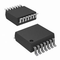
IC RTC/CLDR TEMP SNSR 14-TSSOP
Manufacturer
Intersil
Type
Clock/Calendarr
Datasheet
1.ISL12023IVZ.pdf
(28 pages)
Specifications of ISL12023IVZ
Memory Size
1K (128 x 8)
Time Format
HH:MM:SS (12/24 hr)
Date Format
YY-MM-DD-dd
Interface
I²C, 2-Wire Serial
Voltage - Supply
2.7 V ~ 5.5 V
Operating Temperature
-40°C ~ 85°C
Mounting Type
Surface Mount
Package / Case
14-TSSOP
Lead Free Status / RoHS Status
Lead free / RoHS Compliant
Available stocks
Company
Part Number
Manufacturer
Quantity
Price
Company:

Part Number:
ISL12023IVZ
Manufacturer:
Intersil
Quantity:
341


General Purpose User SRAM
The ISL12023 provides 128 bytes of user SRAM. The SRAM
will continue to operate in battery-backup mode. However, it
should be noted that the I
battery-backup mode.
I
The ISL12023 has an I
access to the control and status registers and the user
SRAM. The I
industry I
signal (SDA) and a clock signal (SCL).
Oscillator Compensation
The ISL12023 provides both initial timing correction and
temperature correction due to variation of the crystal
oscillator. Analog and digital trimming control is provided for
initial adjustment, and a temperature compensation function
is provided to automatically correct for temperature drift of
the crystal. Initial values are preset and recalled on initial
power-up for the Initial AT and DT settings (IATR, IDTR),
temperature coefficient (ALPHA), crystal capacitance
(BETA), and the crystal turnover temperature (XTO). These
initial values are typical of units available on the market,
although the user may program specific values after testing
for best accuracy. The function can be enabled/disabled at
any time and can be used in battery mode as well.
Register Descriptions
The battery-backed registers are accessible following a
slave byte of “1101111x” and reads or writes to addresses
[00h:2Fh]. The defined addresses and default values are
described in the Table 1. The battery backed general
purpose SRAM has a different slave address (1010111x), so
it is not possible to read/write that section of memory while
accessing the registers.
REGISTER ACCESS
The contents of the registers can be modified by performing
a byte or a page write operation directly to any register
address.
ADDR. SECTION
2
C Serial Interface
00h
01h
02h
03h
04h
05h
06h
2
C serial bus protocols using a bi-directional data
RTC
2
C serial interface is compatible with other
NAME
REG
MO
DW
MN
HR
SC
DT
YR
2
C serial bus interface that provides
2
C bus is disabled in
11
YR23
MIL
0
0
0
0
0
7
MN22
SC22
YR22
6
0
0
0
0
TABLE 1. REGISTER MEMORY MAP
MN21
SC21
HR21
DT21
YR21
5
0
0
ISL12023
MN20
MO20
SC20
HR20
DT20
YR20
4
0
BIT
The registers are divided into 8 sections. They are:
10. Crystal ALPHA at high temperature, ALPHA_H (1 byte):
11. Scratch Pad (2 bytes): Address 2Eh and 2Fh
Write capability is allowable into the RTC registers (00h to
06h) only when the WRTC bit (bit 6 of address 08h) is set to
“1”. A multi-byte read or write operation should be limited to
one section per operation for best RTC time keeping
performance. When the previous ddress is 2Fh, the next
address will wrap around to 00h.
A register can be read by performing a random read at any
address at any time. This returns the contents of that register
location. Additional registers are read by performing a
sequential read. For the RTC and Alarm registers, the read
instruction latches all clock registers into a buffer, so an
update of the clock does not change the time being read. At
the end of a read, the master supplies a stop condition to
end the operation and free the bus. After a read, the address
remains at the previous address +1 so the user can execute
a current address read and continue reading the next
register.
It is not necessary to set the WRTC bit prior to writing into
the control and status, alarm, and user SRAM registers.
1. Real Time Clock (7 bytes): Address 00h to 06h.
2. Control and Status (13 bytes): Address 07h to 0Fh and
3. Alarm (6 bytes): Address 10h to 15h.
4. Time Stamp for Battery Status (5 bytes): Address 16h to
5. Time Stamp for V
6. Daylight Saving Time (8 bytes): 20h to 27h.
7. Temperature (2 bytes): 28h to 29h
8. Crystal Net PPM Correction, NPPM (2 bytes): 2Ah, 2Bh
9. Crystal Turnover Temperature, XT0 (1 byte): 2Ch
MO13
MN13
SC13
HR13
DT13
YR13
2Ah to 2Dh.
1Ah.
1Fh.
2Dh
3
0
MN12
MO12
SC12
HR12
DT12
YR12
DW2
2
DD
MO11
MN11
HR11
SC11
DT11
YR11
DW1
1
Status (5 bytes): Address 1Bh to
MO10
MN10
HR10
SC10
DT10
YR10
DW0
0
RANGE
0 to 59
0 to 59
0 to 23
1 to 31
1 to 12
0 to 99
0 to 6
June 24, 2009
DEFAULT
FN6682.2
00h
00h
00h
01h
01h
00h
00h
Related parts for ISL12023IVZ
Image
Part Number
Description
Manufacturer
Datasheet
Request
R

Part Number:
Description:
Intersil Corporation [CMOS Serial Controller Interface]
Manufacturer:
Intersil Corporation
Datasheet:
Part Number:
Description:
Manufacturer:
Intersil Corporation
Datasheet:
Part Number:
Description:
357-036-542-201 CARDEDGE 36POS DL .156 BLK LOPRO
Manufacturer:
Intersil Corporation
Datasheet:
Part Number:
Description:
1024-Word x 4-Bit LSI Static RAM
Manufacturer:
Intersil Corporation
Datasheet:
Part Number:
Description:
General Purpose NPN Transistor Arrays FN341.4
Manufacturer:
Intersil Corporation
Datasheet:
Part Number:
Description:
CMOS 16-Bit Microprocessor
Manufacturer:
Intersil Corporation
Datasheet:
Part Number:
Description:
Manufacturer:
Intersil Corporation
Datasheet:
Part Number:
Description:
Manufacturer:
Intersil Corporation
Datasheet:
Part Number:
Description:
Manufacturer:
Intersil Corporation
Datasheet:
Part Number:
Description:
Manufacturer:
Intersil Corporation
Datasheet:
Part Number:
Description:
CMOS 6-Bit Latch and Decoder Memory Interfaces
Manufacturer:
Intersil Corporation
Datasheet:
Part Number:
Description:
CA3046General Purpose NPN Transistor Arrays
Manufacturer:
Intersil Corporation
Datasheet:
Part Number:
Description:
Manufacturer:
Intersil Corporation
Datasheet:
Part Number:
Description:
TR909 DLC/FLC SLIC with Low Power Standby
Manufacturer:
Intersil Corporation
Datasheet:
Part Number:
Description:
Manufacturer:
Intersil Corporation
Datasheet: