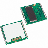
DS1554WP-120+ Maxim Integrated Products, DS1554WP-120+ Datasheet - Page 7

DS1554WP-120+
Manufacturer Part Number
DS1554WP-120+
Description
IC RTC RAM Y2K 3.3V 120NS 34-PCM
Manufacturer
Maxim Integrated Products
Type
Clock/Calendar/NVSRAM/Y2Kr
Datasheet
1.DS1554P-70.pdf
(18 pages)
Specifications of DS1554WP-120+
Memory Size
256K (32K x 8)
Time Format
HH:MM:SS (24 hr)
Date Format
YY-MM-DD-dd
Interface
Parallel
Voltage - Supply
3 V ~ 3.6 V
Operating Temperature
0°C ~ 70°C
Mounting Type
Surface Mount
Package / Case
34-PowerCap™ Module
Lead Free Status / RoHS Status
Lead free / RoHS Compliant
Table 2. Register Map
CLOCK OSCILLATOR CONTROL
The Clock oscillator may be stopped at any time. To increase the shelf life of the backup lithium battery
source, the oscillator can be turned off to minimize current drain from the battery. The OSC bit is the
MSB of the Seconds Register (B7 of 7FF9h). Setting it to a 1 stops the oscillator, setting to a 0 starts the
oscillator. The DS1554 is shipped from Maxim with the clock oscillator turned off, OSC bit set to a 1.
READING THE CLOCK
When reading the RTC data, it is recommended to halt updates to the external set of double-buffered RTC
Registers. This puts the external registers into a static state allowing data to be read without register
values changing during the read process. Normal updates to the internal registers continue while in this
state. External updates are halted when a 1 is written into the read bit, B6 of the Control Register (7FF8h).
As long as a 1 remains in the Control Register read bit, updating is halted. After a halt is issued, the
registers reflect the RTC count (day, date, and time) that was current at the moment the halt command
was issued. Normal updates to the external set of registers will resume within 1 second after the read bit is
set to a 0 for a minimum of 500 s. The read bit must be a zero for a minimum of 500 s to ensure the
external registers will be updated.
ADDRESS
X = Unused, Read/Writeable under Write and Read Bit Control
Y = Unused, Read/Writeable without Write and Read Bit Control
FT = Frequency Test Bit
OSC = Oscillator Start/Stop Bit
W = Write Bit
R = Read Bit
WDS = Watchdog Steering Bit
BMB0 to BMB4 = Watchdog Multiplier Bits
7FFDh
7FFAh
7FFEh
7FFCh
7FFBh
7FFFh
7FF9h
7FF8h
7FF7h
7FF6h
7FF5h
7FF4h
7FF3h
7FF2h
7FF1h
7FF0h
WDS
AM4
AM3
AM2
AM1
OSC
WF
AE
B
W
X
X
X
X
X
Y
7
BMB4
AF
FT
B
X
X
X
Y
Y
Y
Y
R
6
10 Year
10 Seconds
10 Seconds
10 Minutes
10 Minutes
BMB3
ABE
B
X
X
Y
0
10 Century
5
10 Hours
10 Hour
10 Date
10 Date
Month
BMB2
BLF
B
10
DATA
X
Y
Y
4
BMB1
B
DS1554 256k, Nonvolatile, Y2K-Compliant Timekeeping RAM
X
Y
Y
0
7 of 18
3
AE = Alarm Flag Enable
ABE = Alarm in Battery-Backup Mode Enable
AM1-AM4 = Alarm Mask Bits
WF = Watchdog Flag
AF = Alarm Flag
0 = 0 (Read Only)
BLF = Battery Low Flag
RB0 to RB1 = Watchdog Resolution Bits
BMB0
Minutes
Seconds
Minutes
Seconds
Century
B
Y
Y
Month
0
Hours
Hour
Year
Date
Date
2
Day
RB1
B
Y
Y
0
1
RB0
B
Y
Y
0
0
Alarm Seconds
Alarm Minutes
Alarm Hours
FUNCTION/RANGE
Alarm Date
Watchdog
Interrupts
Minutes
Seconds
Control
Unused
Month
Flags
Hour
Year
Date
Day
00-99
01-12
01-31
01-07
00-23
00-59
00-59
00-39
01-31
00-23
00-59
00-59
—
—
—
—


