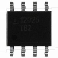
ISL12025IBZ Intersil, ISL12025IBZ Datasheet - Page 16

ISL12025IBZ
Manufacturer Part Number
ISL12025IBZ
Description
IC RTC/CALENDAR EEPROM 8-SOIC
Manufacturer
Intersil
Type
Clock/Calendar/Supervisor/EEPROMr
Specifications of ISL12025IBZ
Memory Size
4K (512 x 8)
Time Format
HH:MM:SS (12/24 hr)
Date Format
YY-MM-DD-dd
Interface
I²C, 2-Wire Serial
Voltage - Supply
2.7 V ~ 5.5 V
Operating Temperature
-40°C ~ 85°C
Mounting Type
Surface Mount
Package / Case
8-SOIC (3.9mm Width)
Bus Type
Serial (I2C)
Operating Supply Voltage (typ)
3.3V
Operating Supply Voltage (max)
5.5V
Operating Supply Voltage (min)
2.7V
Operating Temperature Classification
Industrial
Operating Temperature (max)
85C
Operating Temperature (min)
-40C
Pin Count
8
Mounting
Surface Mount
Clock Format
HH
Clock Ic Type
RTC
Interface Type
I2C, Serial
Memory Configuration
512 X 8
Supply Voltage Range
2.7V To 5.5V
Digital Ic Case Style
SOIC
Rohs Compliant
Yes
Lead Free Status / RoHS Status
Lead free / RoHS Compliant
Watchdog Timer Restart
The Watchdog Timer is started by a falling edge of SDA
when the SCL line is high (START condition). The start
signal restarts the Watchdog timer counter, resetting the
period of the counter back to the maximum. If another
START fails to be detected prior to the watchdog timer
expiration, then the RESET pin becomes active for one reset
time out period. In the event that the start signal occurs
during a reset time out period, the start will have no effect.
When using a single START to refresh Watchdog timer, a
STOP condition should be followed to reset the device back
to Standby Power Mode (see Figure 3).
Low Voltage Reset (LVR) Operation
When a power failure occurs, a voltage comparator
compares the level of the V
voltage (V
below V
V
V
Power-up and power-down waveforms are shown in
Figure 4. The LVR circuit is to be designed so the RESET
signal is valid down to V
When the LVR signal is active, unless the part has been
switched into the Battery Backup Mode
in-progress non-volatile write cycle is unaffected, allowing a
non-volatile write to continue as long as possible (down to
the Reset Valid Voltage). The LVR signal, when active, will
terminate any in-progress communications to the device and
prevents new commands from disrupting any current write
operations. See “I
Backup and LVR Operation” on page 23.
Serial Communication
Interface Conventions
The device supports the I
DD
RESET
WD1
line rises above V
1
1
0
0
RESET
, then the RESET output will remain asserted low.
RESET
. The reset pulse will timeout 250ms after the
), then generates a RESET pulse if it is
2
WD0
C Communications During Battery
1
0
1
0
RESET
DD
SDA
SCL
2
TABLE 6.
C Protocol.
DD
= 1.0V.
16
. If the V
line versus a preset threshold
FIGURE 16. VALID DATA CHANGES ON THE SDA BUS
DD
DURATION
,
the completion of an
disabled
250ms
750ms
1.75s
remains below
DATA STABLE
ISL12025
DATA CHANGE
Clock and Data
Data states on the SDA line can change only during SCL
LOW. SDA state changes during SCL HIGH are reserved for
indicating start and stop conditions (see Figure 16).
Start Condition
All commands are preceded by the start condition, which is a
HIGH to LOW transition of SDA when SCL is HIGH. The
device continuously monitors the SDA and SCL lines for the
start condition and will not respond to any command until
this condition has been met (see Figure 17).
Stop Condition
All communications must be terminated by a stop condition,
which is a LOW to HIGH transition of SDA when SCL is
HIGH. The stop condition is also used to place the device
into the Standby Power Mode after a read sequence. A stop
condition can only be issued after the transmitting device
has released the bus (see Figure 17).
Acknowledge
Acknowledge is a software convention used to indicate
successful data transfer. The transmitting device, either
master or slave, will release the bus after transmitting 8-bits.
During the ninth clock cycle, the receiver will pull the SDA
line LOW to acknowledge that it received the 8-bits of data
(see Figure 18).
The device will respond with an acknowledge after
recognition of a start condition and if the correct Device
Identifier and Select bits are contained in the Slave Address
Byte. If a write operation is selected, the device will respond
with an acknowledge after the receipt of each subsequent
8-bit word. The device will not acknowledge if the slave
address byte is incorrect.
In the read mode, the device will transmit eight bits of data,
release the SDA line, then monitor the line for an
acknowledge. If an acknowledge is detected and no stop
condition is generated by the master, the device will continue
to transmit data. The device will terminate further data
transmissions if an acknowledge is not detected. The master
must then issue a stop condition to return the device to
Standby Power Mode and place the device into a known
state.
DATA STABLE
August 13, 2008
FN6371.3


