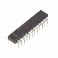
DS12885N+ Maxim Integrated Products, DS12885N+ Datasheet - Page 17

DS12885N+
Manufacturer Part Number
DS12885N+
Description
IC RTC W/RAM 128 BYTE 24-DIP
Manufacturer
Maxim Integrated Products
Type
Clock/Calendar/NVSRAMr
Datasheet
1.DS12885N.pdf
(22 pages)
Specifications of DS12885N+
Memory Size
114B
Time Format
HH:MM:SS (12/24 hr)
Date Format
YY-MM-DD-dd
Interface
Parallel
Voltage - Supply
4.5 V ~ 5.5 V
Operating Temperature
-40°C ~ 85°C
Mounting Type
Through Hole
Package / Case
24-DIP (0.600", 15.24mm)
Function
Clock/Calendar/Alarm
Rtc Memory Size
114 Byte
Supply Voltage (max)
5.5 V
Supply Voltage (min)
4.5 V
Maximum Operating Temperature
+ 85 C
Minimum Operating Temperature
- 40 C
Mounting Style
Through Hole
Rtc Bus Interface
Multiplexed
Supply Current
15 mA
Lead Free Status / RoHS Status
Lead free / RoHS Compliant
Bit 7: Interrupt Request Flag (IRQF). This bit is set to
1 when any of the following are true:
Any time the IRQF bit is 1, the IRQ pin is driven low.
This bit can be cleared by reading Register C or with a
RESET.
Bit 6: Periodic Interrupt Flag (PF). This bit is read-
only and is set to 1 when an edge is detected on the
selected tap of the divider chain. The RS3 through RS0
bits establish the periodic rate. PF is set to 1 indepen-
dent of the state of the PIE bit. When both PF and PIE
are 1s, the IRQ signal is active and sets the IRQF bit.
This bit can be cleared by reading Register C or with a
RESET.
MSB
MSB
Bit 7: Valid RAM and Time (VRT). This bit indicates
the condition of the battery connected to the V
This bit is not writeable and should always be 1 when
read. If a 0 is ever present, an exhausted internal lithi-
um energy source is indicated and both the contents of
BIT 7
BIT 7
IRQF
PF = PIE = 1
AF = AIE = 1
UF = UIE = 1
VRT
BIT 6
BIT 6
PF
0
BIT 5
BIT 5
AF
0
____________________________________________________________________
BAT
BIT 4
BIT 4
UF
0
pin.
the RTC data and RAM data are questionable. This bit
is unaffected by RESET.
Bits 6 to 0: Unused. The remaining bits of Register D
are not usable. They cannot be written and they always
read 0.
Bit 5: Alarm Interrupt Flag (AF). A 1 in the AF bit indi-
cates that the current time has matched the alarm time.
If the AIE bit is also 1, the IRQ pin goes low and a 1
appears in the IRQF bit. This bit can be cleared by
reading Register C or with a RESET.
Bit 5: Update-Ended Interrupt Flag (UF). This bit is
set after each update cycle. When the UIE bit is set to
1, the 1 in UF causes the IRQF bit to be a 1, which
asserts the IRQ pin. This bit can be cleared by reading
Register C or with a RESET.
Bits 3 to 0: Unused. These bits are unused in Register
C. These bits always read 0 and cannot be written.
BIT 3
BIT 3
0
0
Real-Time Clocks
BIT 2
BIT 2
0
0
Control Register C
BIT 1
Control Register D
BIT 1
0
0
BIT 0
BIT 0
0
0
LSB
LSB
17


