DS4M125P+33 Maxim Integrated Products, DS4M125P+33 Datasheet - Page 2
DS4M125P+33
Manufacturer Part Number
DS4M125P+33
Description
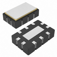
IC OSC CLOCK 125MHZ 10-LCCC
Manufacturer
Maxim Integrated Products
Type
Clock Oscillatorr
Datasheet
1.DS4M133D33.pdf
(7 pages)
Specifications of DS4M125P+33
Frequency
125MHz
Voltage - Supply
3.135 V ~ 3.465 V
Current - Supply
74mA
Operating Temperature
-40°C ~ 85°C
Package / Case
10-LCCC
Lead Free Status / RoHS Status
Lead free / RoHS Compliant
Count
-


ABSOLUTE MAXIMUM RATINGS
Power-Supply Voltage Range (V
Continuous Power Dissipation (T
Operating Temperature Range ...........................-40°C to +85°C
Junction Temperature ......................................................+125°C
3.3V Margining Clock Oscillator with
LVPECL/LVDS Output
Stresses beyond those listed under “Absolute Maximum Ratings” may cause permanent damage to the device. These are stress ratings only, and functional
operation of the device at these or any other conditions beyond those indicated in the operational sections of the specifications is not implied. Exposure to
absolute maximum rating conditions for extended periods may affect device reliability.
ELECTRICAL CHARACTERISTICS
(V
2
Operating Voltage Range
Operating Current
Inactive Current
OUTPUT FREQUENCY SPECIFICATIONS
Frequency
Frequency Stability
Frequency Stability Over
Temperature
Initial Tolerance
Frequency Change Due to V
Frequency Change Due to Load
Variation
Aging (15 Years)
Phase Jitter
Accumulated Deterministic Jitter
Due to Reference Spurs
Accumulated Deterministic Jitter
Due to Power-Supply Noise
Startup Time
Frequency Switch Time
Input-Voltage High (OE)
CC
_______________________________________________________________________________________
= 3.135V to 3.465V, T
PARAMETER
DS4M125
DS4M133
DS4M200
A
= -40°C to +85°C, unless otherwise noted.) (Notes 1, 2)
CC
CC
A
= +70°C) ...................330mW
) .....................-0.3V to +4.0V
SYMBOL
I
f
f
t
f
CC_OEZ
I
TOTAL/
INITIAL
SWITCH
I
LOAD/
I
CC_PU
f
f
J
t
CC_PI
f
CC_D
TEMP
AGING
V
STRT
V
VCC
RMS
f
CC
O
IH
/f
f
/f
/f
f
O
O
V
(Note 1)
LVDS, output loaded or unloaded
LVPECL, output unloaded
LVPECL, output loaded
V
MS = 0, OE = 1
MS = 0, OE = 1
MS = 0, OE = 1
Over temperature range, aging, load,
supply, and initial tolerance (Note 3)
V
V
V
±10% variation in termination
resistance
Integrated phase RMS; 12kHz to 80MHz,
V
No margin 155.52MHz output
10kHz
100kHz (Note 4)
200kHz (Note 4)
1MHz (Note 4)
(Note 5)
OE
CC
CC
CC
CC
= 3.3V
= 3.3V, T
= 3.3V ±5%
= 3.3V, T
= V
IL
CONDITIONS
A
A
Storage Temperature Range ...............................-55°C to +85°C
Soldering Temperature
= +25°C
= +25°C
(3 passes max of reflow)..........................................Refer to the
IPC/JEDEC J-STD-020 Specification.
3.135
0.7 x
MIN
V
-50
-35
-3
-7
CC
133.33
< 0.9
TYP
12.9
26.3
20.1
±20
125
200
3.3
0.6
6.4
1.0
0.5
±1
52
49
74
52
3.465
MAX
+50
+35
100
V
+3
+7
75
70
85
CC
UNITS
ppm/V
MHz
ppm
ppm
ppm
ppm
ppm
mA
mA
ms
ms
ps
ps
ps
V
V
Related parts for DS4M125P+33
Image
Part Number
Description
Manufacturer
Datasheet
Request
R

Part Number:
Description:
3.3V Margining Clock Oscillator with LVPECL/LVDS Output
Manufacturer:
MAXIM [Maxim Integrated Products]
Datasheet:

Part Number:
Description:
MAX7528KCWPMaxim Integrated Products [CMOS Dual 8-Bit Buffered Multiplying DACs]
Manufacturer:
Maxim Integrated Products
Datasheet:
Part Number:
Description:
Single +5V, fully integrated, 1.25Gbps laser diode driver.
Manufacturer:
Maxim Integrated Products
Datasheet:
Part Number:
Description:
Single +5V, fully integrated, 155Mbps laser diode driver.
Manufacturer:
Maxim Integrated Products
Datasheet:
Part Number:
Description:
VRD11/VRD10, K8 Rev F 2/3/4-Phase PWM Controllers with Integrated Dual MOSFET Drivers
Manufacturer:
Maxim Integrated Products
Datasheet:
Part Number:
Description:
Highly Integrated Level 2 SMBus Battery Chargers
Manufacturer:
Maxim Integrated Products
Datasheet:
Part Number:
Description:
Current Monitor and Accumulator with Integrated Sense Resistor; ; Temperature Range: -40°C to +85°C
Manufacturer:
Maxim Integrated Products
Part Number:
Description:
TSSOP 14/A�/RS-485 Transceivers with Integrated 100O/120O Termination Resis
Manufacturer:
Maxim Integrated Products
Part Number:
Description:
TSSOP 14/A�/RS-485 Transceivers with Integrated 100O/120O Termination Resis
Manufacturer:
Maxim Integrated Products
Part Number:
Description:
QFN 16/A�/AC-DC and DC-DC Peak-Current-Mode Converters with Integrated Step
Manufacturer:
Maxim Integrated Products
Part Number:
Description:
TDFN/A/65V, 1A, 600KHZ, SYNCHRONOUS STEP-DOWN REGULATOR WITH INTEGRATED SWI
Manufacturer:
Maxim Integrated Products
Part Number:
Description:
Integrated Temperature Controller f
Manufacturer:
Maxim Integrated Products
Part Number:
Description:
SOT23-6/I�/45MHz to 650MHz, Integrated IF VCOs with Differential Output
Manufacturer:
Maxim Integrated Products
Part Number:
Description:
SOT23-6/I�/45MHz to 650MHz, Integrated IF VCOs with Differential Output
Manufacturer:
Maxim Integrated Products
Part Number:
Description:
EVALUATION KIT/2.4GHZ TO 2.5GHZ 802.11G/B RF TRANSCEIVER WITH INTEGRATED PA
Manufacturer:
Maxim Integrated Products