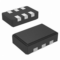
CY2XF24FLXIT Cypress Semiconductor Corp, CY2XF24FLXIT Datasheet

CY2XF24FLXIT
Specifications of CY2XF24FLXIT
Related parts for CY2XF24FLXIT
CY2XF24FLXIT Summary of contents
Page 1
... V Power Power SS Cypress Semiconductor Corporation Document Number: 001-53146 Rev. *D PRELIMINARY High Performance LVPECL Oscillator with Frequency Margining - I Functional Description The CY2XF24 is a high-performance and high-frequency XO. It uses a Cypress-proprietary low-noise PLL to synthesize the frequency from an integrated crystal. The output frequency can be changed using the I frequency margin testing in applications ...
Page 2
Contents Features............................................................................. 1 Functional Description..................................................... 1 Logic Block Diagram........................................................ 1 Pinouts .............................................................................. 1 Contents ............................................................................ 2 Standard and Application-Specific Factory Configurations .................................................... 3 Functional Description..................................................... 3 Configuration Software.................................................... 3 Programming Description ............................................... 3 Field-Programmable CY2XF24F ................................. 3 Factory-Configured CY2XF24 ..................................... ...
Page 3
Standard and Application-Specific Factory Configurations Part Number Output Frequency CY2XF24LXI625T 78.125 MHz 156.25 MHz 312.50 MHz 625.00 MHz (default) Functional Description The CY2XF24 is a PLL-based high-performance clock generator. It uses an internal crystal oscillator as a reference, and outputs ...
Page 4
Factory-Configured CY2XF24 For ready-to-use devices, the CY2XF24 is available with no field programming required. Pre-configured devices (see and Application-Specific Factory Configurations) are available for samples or orders request for a custom configuration can be made. All requests are ...
Page 5
Write Operations Writing Individual Bytes A valid write operation must have a full 8-bit register address after the device address word from the master, which is followed by an acknowledge bit from the slave (SDA = 0/LOW). The next eight ...
Page 6
Bit SDA Write 1 Bit Slave R ACK Multiple 7-bit 8-bit Contiguous Device Register Registers Address Address (XXH) Start Signal 1 Bit 1 Bit SDA Read Slave ACK R Current 7-bit 8-bit Device Register Address ...
Page 7
Figure 7. Frame Format (Device Address, R/W, Register Address, Register Data) SDA + START DA6 DA5 DA0 R/W + SCLK Absolute Maximum Conditions Parameter Description V Supply voltage DD [2] V Input voltage Temperature, storage S T ...
Page 8
DC Electrical Characteristics Parameter Description V Output low voltage (SDA) OLS V Input high voltage IH V Input low voltage IL I Input high current (SDA) IH0 I Input high current (SCLK) IH1 I Input low current (SDA) IL0 I ...
Page 9
I C Bus Timing Specifications 2 The I C Bus Timing Specifications for part CY2XF24 are as follows Parameter f SCLK frequency SCLK t Start mode time from SDA LOW to SCLK LOW HD:STA t SCLK LOW period LOW ...
Page 10
Figure 9. 2.5-V Supply and Termination to V 0.9 0.8 0.7 0.6 0.5 0.4 0 100 200 300 400 Frequency (MHz) Figure 10. 3.3-V Supply and Termination to V 0.9 0.8 0.7 0.6 0.5 0.4 0 100 200 300 400 ...
Page 11
Measurement Definitions CLK CLK# CLK CLK# Termination Circuits CLK 50Ω 50Ω CLK# Document Number: 001-53146 Rev. *D PRELIMINARY Figure 11. Output DC Parameters V OD Figure 12. Duty Cycle Timing PERIOD Figure 13. Output Rise and Fall ...
Page 12
... Ordering Information Part Number Configuration Pb-free CY2XF24FLXCT Field-programmable CY2XF24FLXIT Field-programmable [9] CY2XF24LXI625T Field-programmable Some product offerings are factory-programmed customer-specific devices with customized part numbers. The Configurations table shows the available device types, but not complete part numbers. Contact your local Cypress FAE or sales representative for more information ...
Page 13
Package Drawings and Dimensions Figure 15. 6-Pin 3.2x5.0 mm Ceramic LCC LZ06A . Acronyms Table 5. Acronyms Used in this Document Acronym Description ESD electrostatic discharge FAE field application engineer HBM human body model JEDEC joint electron devices engineering council ...
Page 14
Document History Page Document Title: CY2XF24 High Performance LVPECL Oscillator with Frequency Margining - I2C Control Document Number: 001-53146 Orig. of Submission Revision ECN Change ** 2704379 KVM/PYRS *A 2718898 WWZ *B 2761926 KVM *C 2896548 KVM *D 2973338 CXQ ...
Page 15
... Cypress against all charges. Any Source Code (software and/or firmware) is owned by Cypress Semiconductor Corporation (Cypress) and is protected by and subject to worldwide patent protection (United States and foreign), United States copyright laws and international treaty provisions. Cypress hereby grants to licensee a personal, non-exclusive, non-transferable license to copy, use, modify, create derivative works of, and compile the Cypress Source Code and derivative works for the sole purpose of creating custom software and or firmware in support of licensee product to be used only in conjunction with a Cypress integrated circuit as specified in the applicable agreement ...


