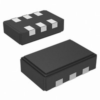
CY2XF32FLXCT Cypress Semiconductor Corp, CY2XF32FLXCT Datasheet - Page 2

CY2XF32FLXCT
Manufacturer Part Number
CY2XF32FLXCT
Description
IC XTAL OSC CMOS 6CLCC
Manufacturer
Cypress Semiconductor Corp
Datasheet
1.CY2XF32FLXCT.pdf
(9 pages)
Specifications of CY2XF32FLXCT
Pll
Yes
Input
Crystal
Output
CMOS
Number Of Circuits
1
Ratio - Input:output
1:1
Differential - Input:output
No/No
Frequency - Max
200MHz
Divider/multiplier
Yes/No
Voltage - Supply
*
Operating Temperature
*
Mounting Type
Surface Mount
Package / Case
6-CLCC
Frequency
*
Count
*
Operating Supply Voltage (typ)
2.5/3.3
Output Level
CMOS
Symmetry Max
55%
Operating Temp Range
0C to 70C
Screening Level
Commercial
Load Capacitance
15pF
Lead Free Status / RoHS Status
Lead free / RoHS Compliant
Table 1. Pin Definitions - 6 Pin Ceramic LCC
Functional Description
The FS0 and FS1 pins select between four different output
frequencies, as shown in
common application for this feature. One frequency is used for
the standard operating mode of the device, while the other
frequencies are available for margin testing, either during
product development or in system manufacturing test.
Table 2. Frequency Select
When changing the output frequency, the frequency transition is
not guaranteed to be smooth. There can be frequency excur-
sions beyond the start frequency and the new frequency.
Glitches and runt pulses are possible, and time must be allowed
for the PLL to relock.
Pin 1 is programmed to function as either OE (output enable) or
PD# (power down, active low). The OE function is used to enable
or disable the CLK output very quickly, but it does not reduce
core power consumption. The PD# function puts the device into
a low power state, but the wake up takes longer because the PLL
must reacquire lock. Details are shown in
Table 3. Output Enable Operation
Document Number: 001-53147 Rev. *C
1
2, 5
4
6
3
Pin
FS1
OE
0
1
0
0
1
1
FS1, FS0
OE/PD#
CLK
VDD
VSS
Name
PLL & Xtal Oscillator
FS0
0
1
0
1
CMOS Input
CMOS Input
CMOS Output
Power
Power
Active
Active
I/O Type
Table
Frequency 0
Frequency 1
Frequency 2
Frequency 3
2. Frequency margining is a
Output Frequency
Output Enable or Power Down: Functionality is a programming option; see
Table 4
Frequency Select.
Clock Output.
Supply Voltage: 2.5V or 3.3V.
Ground.
Table 3
Output Buffer
for details.
PRELIMINARY
and
Off
On
Table
4.
Table 4. Power Down Operation
Programming Description
The CY2XF32 is a programmable device. Before being used in
an application, it must be programmed with the output
frequencies and other variables described in a later section. Two
different device types are available, each with its own
programming flow. They are described below.
Field Programmable CY2XF32F
Field programmable devices are shipped unprogrammed and
must be programmed before being installed on a printed circuit
board (PCB). Customers use CyberClocks™ Online Software to
specify the device configuration and generate a JEDEC
(extension .jed) programming file. Programming of samples and
prototype quantities is available using a Cypress programmer.
Third party vendors manufacture programmers for small to large
volume applications. Cypress’s value added distribution partners
also provide programming services. Field programmable
devices are designated with an “F” in the part number. They are
intended for quick prototyping and inventory reduction. The
CY2XF32 is one time programmable (OTP).
The software is located at
Factory Configured CY2XF32
For ready-to-use devices, the CY2XF32 is available with no field
programming required. All requests are submitted to the local
Cypress Field Application Engineer (FAE) or sales represen-
tative. After the request is processed, the user receives a new
part number, samples, and data sheet with the programmed
values. This part number is used for additional sample requests
and production orders.
PD#
0
1
Description
PLL & Xtal Oscillator
Active
Off
www.cyberclocksonline.com.
Output Buffer
Table 3
CY2XF32
Off
On
Page 2 of 9
and
[+] Feedback


