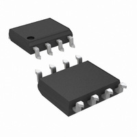
LMC555CMX/NOPB National Semiconductor, LMC555CMX/NOPB Datasheet - Page 5

LMC555CMX/NOPB
Manufacturer Part Number
LMC555CMX/NOPB
Description
IC TIMER CMOS 8-SOIC
Manufacturer
National Semiconductor
Type
555 Type, Timer/Oscillator (Single)r
Datasheet
1.LMC555CMXNOPB.pdf
(12 pages)
Specifications of LMC555CMX/NOPB
Frequency
3MHz
Voltage - Supply
2 V ~ 15 V
Current - Supply
150µA
Operating Temperature
-40°C ~ 85°C
Package / Case
8-SOIC (3.9mm Width)
Lead Free Status / RoHS Status
Lead free / RoHS Compliant
Count
-
Other names
LMC555CMX
LMC555CMXTR
LMC555CMXTR
Available stocks
Company
Part Number
Manufacturer
Quantity
Price
Part Number:
LMC555CMX/NOPB
Manufacturer:
TI/德州仪器
Quantity:
20 000
Application Information
MONOSTABLE OPERATION
In this mode of operation, the timer functions as a one-shot
(Figure
by internal circuitry. Upon application of a negative trigger
pulse of less than 1/3 V
is set which both releases the short circuit across the capac-
itor and drives the output high.
The voltage across the capacitor then increases exponential-
ly for a period of t
output stays high, at the end of which time the voltage equals
2/3 V
discharges the capacitor and drives the output to its low state.
Figure 2
eration. Since the charge and the threshold level of the com-
parator are both directly proportional to supply voltage, the
timing internal is independent of supply.
V
TIME = 0.1 ms/Div.
R
C = 0.01 µF
Reset overrides Trigger, which can override threshold. There-
fore the trigger pulse must be shorter than the desired t
minimum pulse width for the Trigger is 20ns, and it is 400ns
for the Reset. During the timing cycle when the output is high,
the further application of a trigger pulse will not effect the cir-
CC
A
= 9.1 kΩ
= 5V
S
. The comparator then resets the flip-flop which in turn
1). The external capacitor is initially held discharged
shows the waveforms generated in this mode of op-
FIGURE 2. Monostable Waveforms
FIGURE 1. Monostable (One-Shot)
H
Middle Trace: Output 5 V/Div.
Top Trace: Input 5 V/Div.
= 1.1 R
Bottom Trace: Capacitor Voltage 2 V/Div.
S
to the Trigger terminal, the flip-flop
A
C, which is also the time that the
866910
H
866904
. The
5
cuit so long as the trigger input is returned high at least 10µs
before the end of the timing interval. However the circuit can
be reset during this time by the application of a negative pulse
to the reset terminal. The output will then remain in the low
state until a trigger pulse is again applied.
When the reset function is not use, it is recommended that it
be connected to V
Figure 3
for various time delays.
Note: In monstable operation, the trigger should be driven high before the
ASTABLE OPERATION
If the circuit is connected as shown in
Threshold terminals connected together) it will trigger itself
and free run as a multivibrator. The external capacitor
charges through R
the duty cycle may be precisely set by the ratio of these two
resistors.
In this mode of operation, the capacitor charges and dis-
charges between 1/3 V
the charge and discharge times, and therefore the frequency
are independent of the supply voltage.
FIGURE 4. Astable (Variable Duty Cycle Oscillator)
end of timing cycle.
is a nomograph for easy determination of RC values
+
FIGURE 3. Time Delay
A
to avoid any possibility of false triggering.
+ R
S
and 2/3 V
B
and discharges through R
S
. As in the triggered mode,
Figure 4
(Trigger and
www.national.com
B
866911
866905
. Thus


