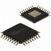
SY55856UHI Micrel Inc, SY55856UHI Datasheet - Page 4

SY55856UHI
Manufacturer Part Number
SY55856UHI
Description
IC DELAY LINE CML 2-CH 32-TQFP
Manufacturer
Micrel Inc
Datasheet
1.SY55856UHG.pdf
(9 pages)
Specifications of SY55856UHI
Function
Delay Generator
Delay To 1st Tap
50pS
Tap Increment
50ps
Available Total Delays
.35ns
Number Of Independent Delays
7
Voltage - Supply
2.3 V ~ 3.6 V
Operating Temperature
-40°C ~ 85°C
Mounting Type
Surface Mount
Package / Case
32-TQFP Exposed Pad, 32-eTQFP, 32-HTQFP, 32-VQFP
Lead Free Status / RoHS Status
Contains lead / RoHS non-compliant
Number Of Taps/steps
-
Lead Free Status / Rohs Status
Not Compliant
Available stocks
Company
Part Number
Manufacturer
Quantity
Price
Micrel, Inc.
Establishing Static Logic Inputs
The true pin of a CML input pair is internally biased to
ground through a 75kΩ resistor. The complement pin of a
CML input pair is internally biased halfway between V
and ground by a voltage divider consisting of two 75kΩ
resistors. To keep a CML input at static logic zero at V
3.0V, leave both inputs unconnected. For V
connect the complement input to V
input unconnected. To make an input static logic one,
connect the true input to V
input unconnected. These are the only safe ways to cause
CML inputs to be at a static value. In particular, no CML
input should be directly connected to ground. All NC pins in
the figures below should be left unconnected.
VT (Variable Threshold) Inputs
Five inputs to SY55856U, CINV, DELAY_SEL, S0, S1, and
S2, are variable threshold inputs. The LVL input determines
Note 1.
M9999-021908
hbwhelp@micrel.com or (408) 955-1690
FUNCTIONAL DESCRIPTION
IN is either the DATA_IN or the CLK_IN input. /IN is either the /
DATA_IN or the /CLK_IN input.
Figure 3a. Logic Switching Threshold
Figure 1. Hard Wiring a Logic "1"
Threshold
Switching
V
CC
Logic
– 0.1V
V
V
TCL
V
NC
CC
CC
V
TCL
IN
/IN
Operating
CC
Range
V
, and leave the complement
CC
– 0.1V
CC
V
and leave the true
CC
Input
LVL
(1)
CC
≤ 3.0V,
CC
CC
>
4
the Voltage threshold that differentiates logic high from logic
low for these five inputs only. If LVL is left unconnected, the
VT inputs will switch at about
whichever is higher. To obtain a logic switching threshold
different from this, the LVL input must be driven with the
actual desired threshold voltage. The user may drive the
LVL pin with any voltage between V
For example, driving LVL with a voltage set at Vcc – 1.3V
causes the VT inputs to accept single ended PECL outputs
and switch appropriately.
threshold will not fall below VTCL Volts. Since driving the
LVL input to ground causes the threshold to be somewhere
between V
user will keep the Voltage at the LVL pin at or above V
(max). Please refer to Figure 3 for clarification.
Note that VT inputs are internally clamped so that the
Figure 3b. Interfacing TTL-to-CML Select
TCL
Figure 2. Hard Wiring a Logic "0"
(CINV, DELAY_SEL, S0, S1, S2)
TTL
Driver
(min) and V
V
CC
VCC
NC
NC
NC
3.0V ≤ V
3
TCL
IN
/IN
CC
IN
/IN
1.10k
909Ω
≤ 3.6V
V
V
(max), it is expected that the
CC
CC
> 3.0V
≤ 3.0V
S0, S1, S2
LVL
CC
V
SY55856
CC
V
– 0.1V and ground.
CC
+
2
GND
(1)
SuperLite™
SY55856U
or V
TCL
TCL
,


