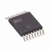
DS1123LE-50+ Maxim Integrated Products, DS1123LE-50+ Datasheet - Page 10

DS1123LE-50+
Manufacturer Part Number
DS1123LE-50+
Description
IC TIMING ELEMENT PROG 16-TSSOP
Manufacturer
Maxim Integrated Products
Datasheet
1.DS1123LE-200.pdf
(14 pages)
Specifications of DS1123LE-50+
Number Of Taps/steps
256
Function
Programmable
Delay To 1st Tap
16.5nS
Tap Increment
0.5nS
Available Total Delays
127.5ns
Voltage - Supply
3 V ~ 3.6 V
Operating Temperature
0°C ~ 70°C
Mounting Type
Surface Mount
Package / Case
16-TSSOP
Lead Free Status / RoHS Status
Lead free / RoHS Compliant
Number Of Independent Delays
-
3.3V, 8-Bit, Programmable Timing Element
Figure 5. Using the Serial Interface
To read the current values stored by the 3-wire
device(s), the latch must be enabled and the value of Q
must be read and then written back to D before the
register is clocked. This causes the current value of the
register to be written back into the DS1123L as it is
being read. This can be accomplished in a couple of
different ways. If the microprocessor has an I/O pin that
is high impedance when set as an input, a feedback
resistor (generally between 1kΩ and 10kΩ) can be
used to write the data on Q back to D as the value is
read (see Figure 5a). If the microprocessor has an
internal pullup on its I/O pins, or only offers separate
input and output pins, the value in the register can still
10
_____________________________________________________________________
A) USING A FEEDBACK RESISTOR WITH AN I/O PIN FOR READING
C) CASCADING MULTIPLE DS1123L'S ON A 3-WIRE BUS
MICROPROCESSOR
MICROPROCESSOR
THE DS1123L
OUTPUT
OUTPUT
OUTPUT
OUTPUT
I/O PIN
I/O PIN
LE
CLK
D
LE
CLK
D
DS1123L
DS1123L
R
FB
U1
P/S
Q
P/S
Q
V
CC
V
CC
B) USING A SEPARATE INPUT PIN TO READ THE DS1123L
be read. The circuit shown in Figure 5b allows the Q
values to read by the microprocessor, which must write
the Q value to D before it can clock the bus to read the
next bit. If the Q values are read without writing them to
D (with the pullup or otherwise), the read is destructive.
A destructive read cycle likely results in an undesirable
change in the delay setting.
Figure 5c shows how to cascade multiple DS1123L’s
onto the same 3-wire bus. One important detail of writ-
ing software for cascaded 3-wire devices is that all the
devices on the bus must be written to or read from dur-
ing each read or write cycle. Attempting to write to only
the first device (U1) would cause the data stored in U1
LE
CLK
D
MICROPROCESSOR
DS1123L
U2
R
OUTPUT
OUTPUT
OUTPUT
FB
INPUT
P/S
Q
V
LE
CLK
D
CC
DS1123L
LE
CLK
D
DS1123L
P/S
Q
U3
V
CC
P/S
Q
V
CC


