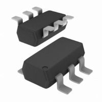
NB2769ASNR2 ON Semiconductor, NB2769ASNR2 Datasheet - Page 2

NB2769ASNR2
Manufacturer Part Number
NB2769ASNR2
Description
IC CLOCK SYNTHESIZR 4MA TSOT-6
Manufacturer
ON Semiconductor
Type
Clock/Frequency Synthesizerr
Datasheet
1.NB2769ASNR2.pdf
(8 pages)
Specifications of NB2769ASNR2
Pll
Yes
Input
CMOS, Crystal
Output
CMOS
Number Of Circuits
1
Ratio - Input:output
1:1
Differential - Input:output
No/No
Frequency - Max
13MHz
Divider/multiplier
Yes/No
Voltage - Supply
2.375 V ~ 3.6 V
Operating Temperature
0°C ~ 70°C
Mounting Type
Surface Mount
Package / Case
SC-74-6
Frequency-max
13MHz
Lead Free Status / RoHS Status
Contains lead / RoHS non-compliant
Available stocks
Company
Part Number
Manufacturer
Quantity
Price
Company:
Part Number:
NB2769ASNR2G
Manufacturer:
NXP
Quantity:
80
Table 1. KEY SPECIFICATIONS
Table 2. PIN DESCRIPTION
XIN/CLKIN
XOUT
Supply Voltages
Frequency Range
Cycle--to--Cycle Jitter
Output Duty Cycle
Modulation Rate Equation
Frequency Deviation
Pin #
1
2
3
4
5
6
XIN/CLKIN
Pin Name
ModOUT
XOUT
V
V
PD
DD
SS
Oscillator
Crystal
Type
O
P
O
P
Description
I
I
Powerdown control pin. Pull low to enable powerdown mode. Connect to V
Crystal connection. If using an external reference, this pin must be left unconnected.
Crystal connection or external reference frequency input. This pin has dual functions. It can be
connected either to an external crystal or an external reference clock.
Power supply for the entire chip.
Spread spectrum clock output.
Ground connection.
XIN/CLKIN
Frequency
Feedback
Divider
Divider
XOUT
PD
For 2.5 V Supply
For 3.3 V Supply
Figure 2. Pin Configuration
1
2
3
Figure 1. Block Diagram
Modulation
http://onsemi.com
Detector
Phase
PD
NB2769A
2
V
6 MHz < CLKIN < 12 MHz
6 MHz < CLKIN < 13 MHz
200 ps (maximum)
45/55% (worst case)
F
1% @ 10 MHz
DD
IN
/256
Loop
Filter
= 3.3 V / 2.5 V
Description
6
5
4
V
V
ModOUT
V
V
V
SS
DD
CO
DD
SS
PLL
Specification
Output
Divider
DD
if not used.
ModOUT


