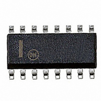
MC100LVEL34DR2 ON Semiconductor, MC100LVEL34DR2 Datasheet - Page 5

MC100LVEL34DR2
Manufacturer Part Number
MC100LVEL34DR2
Description
IC CLOCK GEN 2/4/8 3.3V 16-SOIC
Manufacturer
ON Semiconductor
Series
100LVELr
Type
Clock Generatorr
Datasheet
1.MC100LVEL34DG.pdf
(10 pages)
Specifications of MC100LVEL34DR2
Pll
No
Input
LVDS, NECL, PECL
Output
ECL
Number Of Circuits
1
Ratio - Input:output
1:4
Differential - Input:output
Yes/Yes
Frequency - Max
1.5GHz
Divider/multiplier
Yes/No
Voltage - Supply
±3 V ~ 3.8 V
Operating Temperature
-40°C ~ 85°C
Mounting Type
Surface Mount
Package / Case
16-SOIC (3.9mm Width)
Frequency-max
1.5GHz
Function
Clock Generator
Operating Temperature (max)
85C
Operating Temperature (min)
-40C
Package Type
SOIC
Pin Count
16
Mounting
Surface Mount
Lead Free Status / RoHS Status
Contains lead / RoHS non-compliant
Available stocks
Company
Part Number
Manufacturer
Quantity
Price
Part Number:
MC100LVEL34DR2G
Manufacturer:
ON/安森美
Quantity:
20 000
CLK
CLK
OUTPUT
MR
MR
EN
EN
Q0
Q1
Q2
Q0
Q1
Q2
CLOCK
There are two distinct functional relationships between the Master Reset and Clock:
The EN signal will “freeze” the internal divider flip−flops on the first falling edge of CLK after its assertion. The internal
divider flip−flops will maintain their state during the freeze. When EN is deasserted (LOW), and after the next falling edge
of CLK, then the internal divider flip−flops will “unfreeze” and continue to their next state count with proper phase rela-
tionships.
MR
T
RR
CASE 2: If the MR is deasserted (H−L), after the Clock has transitioned low, the
CASE 1
CASE 1: If the MR is deasserted (H−L), while the Clock is still high, the
outputs will follow the second ensuing clock rising edge.
outputs will follow the third ensuing clock rising edge.
Figure 3. Reset Recovery Time
Figure 2. Timing Diagrams
http://onsemi.com
OUTPUT
CLOCK
5
MR
T
RR
Internal Clock
Internal Clock
Disabled
Disabled
CASE 2
Internal Clock
Internal Clock
Enabled
Enabled


