MC88915FN70 Freescale Semiconductor, MC88915FN70 Datasheet
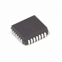
IC DRIVER CLK PLL 70MHZ 28-PLCC

MC88915FN70

Manufacturer Part Number
MC88915FN70
Description
IC DRIVER CLK PLL 70MHZ 28-PLCC
Manufacturer
Freescale Semiconductor
Type
Clock Driver, Fanout Distribution, Multiplexerr
Datasheet

Specifications of MC88915FN70

Pll
Yes
Input
TTL
Output
CMOS, TTL
Number Of Circuits
1
Ratio - Input:output
3:8
Differential - Input:output
No/No
Frequency - Max
70MHz
Divider/multiplier
Yes/Yes
Voltage - Supply
4.75 V ~ 5.25 V
Operating Temperature
0°C ~ 70°C
Mounting Type
Surface Mount
Package / Case
28-PLCC
Frequency-max
70MHz
Lead Free Status / RoHS Status
Contains lead / RoHS non-compliant

Available stocks

Company
Part Number
Manufacturer
Quantity
Price
Part Number:
MC88915FN70
Manufacturer:
MOT
Quantity:
5 510
Part Number:
MC88915FN70
Manufacturer:
IDT, Integrated Device Technology Inc
Quantity:
10 000
Part Number:
MC88915FN70
Manufacturer:
INTEL
Quantity:
382
Part Number:
MC88915FN70
Manufacturer:
MOT
Quantity:
1 000
Part Number:
MC88915FN70
Manufacturer:
MOTOROLA/摩托罗拉
Quantity:
20 000
Part Number:
MC88915FN70R2
Manufacturer:
MOTOROLA
Quantity:
268
Part Number:
MC88915FN70R2
Manufacturer:
Freescale Semiconductor
Quantity:
10 000
Part Number:
MC88915FN70R2
Manufacturer:
MOTOROLA/摩托罗拉
Quantity:
20 000
Low Skew CMOS PLL Clock
Driver
technology to lock its low skew outputs’ frequency and phase
onto an input reference clock. It is designed to provide clock
distribution for high performance PC’s and workstations.
onto a single clock input and distribute it with essentially zero
delay to multiple components on a board. The PLL also allows
the MC88915 to multiply a low frequency input clock and
distribute it locally at a higher (2X) system frequency. Multiple
88915’s can lock onto a single reference clock, which is ideal
for applications when a central system clock must be
distributed synchronously to multiple boards (see Figure 7).
ps skew between their rising edges. The Q5 output is inverted
(180 phase shift) from the “Q” outputs. The 2X_Q output runs
at twice the “Q” output frequency, while the Q/2 runs at 1/2 the
“Q” frequency.
the 2X_Q Fmax specification. The wiring diagrams in Figure 5
detail the different feedback configurations which create
specific input/output frequency relationships. Possible
frequency ratios of the “Q” outputs to the SYNC input are 2:1,
1:1, and 1:2.
divide–by in the feedback path of the PLL. It selects between
divide–by–1 and divide–by–2 of the VCO before its signal
reaches the internal clock distribution section of the chip (see
the block diagram on page 2). In most applications
FREQ_SEL should be held high ( 1). If a low frequency
reference clock input is used, holding FREQ_SEL low ( 2) will
allow the VCO to run in its optimal range (>20 MHz).
high. Pulling the PLL_EN pin low disables the VCO and puts
the 88915 in a static “test mode”. In this mode there is no
frequency limitation on the input clock, which is necessary for
a low frequency board test environment. The second SYNC
input can be used as a test clock input to further simplify
board–level testing (see detailed description on page 11).
in steady–state phase and frequency lock. The LOCK output
will go low if phase–lock is lost or when the PLL_EN pin is low.
Under certain conditions the lock output may remain low, even
though the part is phase–locked. Therefore the LOCK output
signal should not be used to drive any active circuitry; it should
be used for passive monitoring or evaluation purposes only.
Yield Surface Modeling and YSM are trademarks of Motorola, Inc.
1/97
MOTOROLA
SEMICONDUCTOR TECHNICAL DATA
Motorola, Inc. 1997
The MC88915 Clock Driver utilizes phase–locked loop
The PLL allows the high current, low skew outputs to lock
Five “Q” outputs (QO–Q4) are provided with less than 500
The VCO is designed to run optimally between 20 MHz and
The FREQ_SEL pin provides one bit programmable
In normal phase–locked operation the PLL_EN pin is held
A lock indicator output (LOCK) will go high when the loop is
1
Features
FEEDBACK
REF_SEL
V CC (AN)
SYNC[0]
GND(AN)
Five Outputs (QO–Q4) with Output–Output Skew < 500
The phase variation from part–to–part between the SYNC
Input/Output phase–locked frequency ratios of 1:2, 1:1,
Input frequency range from 5MHz – 2X_Q FMAX spec
Additional outputs available at 2X and +2 the system “Q”
All outputs have 36 mA drive (equal high and low) at
Test Mode pin (PLL_EN) provided for low frequency
ps each being phase and frequency locked to the SYNC
input
and FEEDBACK inputs is less than 550 ps (derived from
the t PD specification, which defines the part–to–part
skew)
and 2:1 are available
frequency. Also a Q (180 phase shift) output available
CMOS levels, and can drive either CMOS or TTL inputs.
All inputs are TTL–level compatible
testing. Two selectable CLOCK inputs for test or
redundancy purposes
SYNC[1]
RC1
FREQ_SEL
5
6
7
8
9
10
11
RST
REV 4
12
4
28–Lead Pinout (Top View)
ORDERING INFORMATION
V CC
MC88915FN55
MC88915FN70
13
GND
3
PLASTIC PLCC
CASE 776–02
FN SUFFIX
14
Q5
2
Q0
MC88915
GND
V CC
15
1
PLCC
PLCC
Q4
28
16
Q1
V CC
GND
27
17
2X_Q
26
18
PLL_EN
25
24
23
22
21
20
19
Q/2
GND
Q3
V CC
Q2
GND
LOCK

Related parts for MC88915FN70

MC88915FN70 Summary of contents

Page 1

... Two selectable CLOCK inputs for test or redundancy purposes RST 4 FEEDBACK 5 REF_SEL 6 SYNC[ (AN) 8 RC1 9 GND(AN) 10 SYNC[ FREQ_SEL 1 REV 4 MC88915 GND 2X_Q GND GND PLL_EN 28–Lead Pinout (Top View) FN SUFFIX PLASTIC PLCC CASE 776–02 ORDERING INFORMATION MC88915FN55 PLCC MC88915FN70 PLCC Q/2 GND GND LOCK ...

Page 2

MC88915 FEEDBACK SYNC (0) 0 PHASE/FREQ SYNC (1) 1 REF_SEL PLL_EN RST PIN SUMMARY Pin Name Num I/O 1 SYNC[0] Input Reference clock input 1 SYNC[1] Input Reference clock input 1 REF_SEL Input Chooses reference between sync[0] ...

Page 3

... V 5.25 4.51 4.75 0.44 V 5.25 0.44 5.25 1.0 A 1.5 2 5. 5.25 –88 mA 5.25 1.0 mA Unit Conditions Min Max Unit – 3.0 ns FN70 200 1 200 28.5 50% 25% Guaranteed Minimum MC88915FN70 Unit 55 70 MHz 27.5 35 MHz MOTOROLA ...

Page 4

MC88915 AC ELECTRICAL CHARACTERISTICS ( + 5.0V 5 50pF) Symbol t RISE , t FALL Rise and Fall Times, all Outputs Into a 50 pF, 500 (Outputs) (Between 0.2V ...

Page 5

General AC Specification Notes 1. Several specifications can only be measured when the MC88915 is in phase–locked operation not possible to have the part in phase–lock on ATE (automated test equipment). Statistical characterization techniques were used to guarantee ...

Page 6

MC88915 RC1 EXTERNAL LOOP FILTER 330 R2 0 With the 470K resistor tied in this fashion, the t PD specification measured at the input pins is 2.25ns 1.0ns SYNC INPUT 2.25ns OFFSET FEEDBACK OUTPUT Figure ...

Page 7

Calculation of Total Output–to–Skew between multiple parts (Part–to–Part skew) By combining the t PD specification and the information in Note 5, the worst case output–to–output skew between multiple 88915’s connected in parallel can be calculated. This calculation assumes that ...

Page 8

MC88915 SYNC INPUT (SYNC[1] or SYNC[0 FEEDBACK INPUT Q/2 OUTPUT t SKEWALL Q0 – Q4 OUTPUTS Q5 OUTPUT 2X_Q OUTPUT Figure 4. Output / Input Switching Waveforms and Timing Diagrams (These waveforms represent the hook–up configuration of Figure ...

Page 9

MHz FEEDBACK SIGNAL HIGH RST Q5 FEEDBACK LOW REF_SEL 12.5 MHz INPUT CRYSTAL SYNC[0] MC88915 OSCILLATOR ANALOG V CC EXTERNAL LOOP RC1 FILTER ANALOG GND FQ_SEL Q0 HIGH Figure 5a. Wiring Diagram and Frequency Relationships With Q/2 Output Feed ...

Page 10

MC88915 0.1 F HIGH 10 F LOW FREQ BYPASS Figure 6. Recommended Loop Filter and Analog Isolation Scheme for the MC88915 Notes Concerning Loop Filter and Board Layout Issues 1. Figure 6 shows a loop filter and analog isolation scheme ...

Page 11

CLOCK @ f SYSTEM CLOCK SOURCE DISTRIBUTE CLOCK @ f CLOCK @ 2f AT POINT OF USE Figure 7. Representation of a Potential Multi–Processing Application Utilizing the MC88915 for Frequency Multiplication and Low Board–to–Board Skew MC88915 System Level Testing Functionality ...

Page 12

MC88915 –N– –L– 0.010 (0.250) T L– NOTES: 1. DATUMS –L–, –M–, AND –N– DETERMINED WHERE TOP OF LEAD SHOULDER EXITS PLASTIC BODY AT MOLD PARTING LINE. ...

Page 13

Motorola reserves the right to make changes without further notice to any products herein. Motorola makes no warranty, representation or guarantee regarding the suitability of its products for any particular purpose, nor does Motorola assume any liability arising out of ...

Related keywords