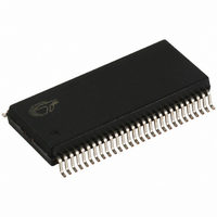
CY28346ZXCT Cypress Semiconductor Corp, CY28346ZXCT Datasheet

CY28346ZXCT
Specifications of CY28346ZXCT
Available stocks
Related parts for CY28346ZXCT
CY28346ZXCT Summary of contents
Page 1
... TCLK is a test clock driven on the XTAL_IN input during test mode driven to a level between 1.0V and 1.8V. If the S2 pin level during power-up state will be latched into the device’s internal state register. Cypress Semiconductor Corporation Document #: 38-07331 Rev. *C • 5/6 copies of 3V66 clocks • ...
Page 2
Pin Description Pin Name PWR 2 XIN 3 XOUT V DD 52, 51, 49, 48, CPUT(0:2 45, 44 CPUC(0:2) 10, 11, 12, 13, PCI(0:6) V DDP 16, 17 PCIF (0: REF ...
Page 3
Two-Wire SMBus Control Interface The two-wire control interface implements a Read/Write slave only interface according to SMBus specification. The device will accept data written to the D2 address and data may read back from address D3. It will not respond ...
Page 4
Byte 2: PCI Clock Control Register (all bits are Read and Write functional) Bit @Pup Pin REF Output Control high strength low strength PCI6 Output Control enabled, 0 ...
Page 5
Byte 6: Silicon Signature Register Bit @Pup Pin Revision = 0001 Vendor Code = 0011 Byte 7: Reserved Register Bit @Pup Pin ...
Page 6
Dial-a-Frequency Features SMBus Dial-a-Frequency feature is available in this device via Byte8 and Byte9 large-value PLL constant that depends on the frequency selection achieved through the hardware selectors (S1, S0). P value may be determined from Table ...
Page 7
Buffer Characteristics Current Mode CPU Clock Buffer Characteristics The current mode output buffer detail and current reference circuit details are contained in the previous table of this data sheet. The following parameters are used to specify output ...
Page 8
Table 4. Host Clock (HCSL) Buffer Characteristics Ro Ros Vout Table 5. CPU Clock Current Select Function Mult0 Board Target Trace/Term Z 0 50Ω 1 50Ω Table 6. Group Timing Relationship and Tolerances Description 3V66 to PCI 48MUSB to 48MDOT ...
Page 9
Special Functions PCI_F and IOAPIC Clock Outputs The PCIF clock outputs are intended to be used, if required, for systems IOAPIC clock functionality. Any two of the PCI_F clock outputs can be used as IOAPIC 33 Mhz clock outputs. They ...
Page 10
PCI_STP# Assertion The PCI_STP# signal is an active LOW input used for synchronous stopping and starting the PCI outputs while the rest of the clock generator continues to function. The set-up CPU_STP# CPUT CPUC CPUT CPUC Table 7. Cypress Clock ...
Page 11
PCI_STP# – Deassertion (transition from logic “0” to logic “1”) The deassertion of the PCI_STP# signal will cause all PCI(0:6) and stoppable PCI_F(0:2) clocks to resume running in a synchronous manner within two PCI clock periods after PCI_STP# transitions to ...
Page 12
PCIF PW RDW N# CPU 133MHz CPU# 133MHz 3V66 66In USB 48MHz REF 14.318MHz Figure 13. Power-down Assertion Timing Waveforms Figure—Buffered Mode PWRDWN# CPUT(0:2) 133MHz CPUC(0:2) 133MHz PCI 33MHz 3V66 USB 48MHz REF 14.318MHz Figure 14. Power-down Assertion Timing ...
Page 13
GMCH 66Buff[0,2] PCIF / APIC 33MHz PCI 33MHz PW RDW N# CPU 133MHz CPU# 133MHz 3V66 66In USB 48MHz REF 14.318MHz Figure 15. Power-down Deassertion Timing Waveforms—Buffered Mode Table 8. PD# Functionality PD# DRCG 1 66M 0 LOW ...
Page 14
Maximum Ratings [5] Input Voltage Relative to V :.............................. V SS Input Voltage Relative DDQ Current Accuracy [6] Parameter Conditions Iout V = nominal (3.30V) DD Iout V = 3.30 ± Parameters (V ...
Page 15
AC Parameters ( 3.3V ±5 DDA Parameter Description T CPU Cycle to Cycle CCJ Jitter T /T CPUT and CPUC Rise R F and Fall Times Rise/Fall Matching DeltaT Rise Time Variation R DeltaT Fall ...
Page 16
AC Parameters ( 3.3V ±5 DDA Parameter Description 66B T 66B(0:2) Duty Cycle 66B(0:2) Rise and Fall R F Times T Any 66B to Any 66B SKEW Skew T 66IN to 66B(0:2) ...
Page 17
AC Parameters ( 3.3V ±5 DDA Parameter Description T /T Output Enable Delay PZL PZH (All Outputs Output disable delay (all PZL PZH outputs) T All Clock Stabilization STABLE from Power-up T Stopclock ...
Page 18
... Figure 17. Clock Generator Power-up/Run State Diagram Ordering Information Part Number CY28346OC CY28346OCT CY28346ZC CY28346ZCT Lead-free CY28346OXC CY28346OXCT CY28346ZXC CY28346ZXCT Document #: 38-07331 Rev Sample Inputs (pins 54,55) VDD3.3 = Off Package Type 56-pin SSOP – Tube 56-pin SSOP – Tape and Reel 56-pin TSSOP – Tube 56-pin TSSOP – ...
Page 19
... Document #: 38-07331 Rev. *C © Cypress Semiconductor Corporation, 2005. The information contained herein is subject to change without notice. Cypress Semiconductor Corporation assumes no responsibility for the use of any circuitry other than circuitry embodied in a Cypress product. Nor does it convey or imply any license under patent or other rights. Cypress products are not warranted nor intended to be used for medical, life support, life saving, critical control or safety applications, unless pursuant to an express written agreement with Cypress ...
Page 20
Document History Page Document Title: CY28346 Clock Synthesizer with Differential CPU Outputs Document Number: 38-07331 REV. ECN NO. Issue Date ** 111653 02/21/02 *A 113983 03/08/02 *B 122897 12/26/02 *C 333314 See ECN Document #: 38-07331 Rev. *C Orig. of ...


