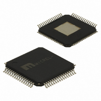
SY89532LHC Micrel Inc, SY89532LHC Datasheet - Page 3

SY89532LHC
Manufacturer Part Number
SY89532LHC
Description
IC SYNTHESIZR LVPECL/LVDS 64TQFP
Manufacturer
Micrel Inc
Series
Precision Edge®r
Type
Clock/Frequency Synthesizerr
Datasheet
1.SY89532LHZ_TR.pdf
(15 pages)
Specifications of SY89532LHC
Pll
Yes
Input
Crystal
Output
LVPECL
Number Of Circuits
1
Ratio - Input:output
1:13
Differential - Input:output
No/Yes
Frequency - Max
500MHz
Divider/multiplier
Yes/No
Voltage - Supply
3 V ~ 3.6 V
Operating Temperature
0°C ~ 85°C
Mounting Type
Surface Mount
Package / Case
64-TQFP Exposed Pad, 64-eTQFP, 64-HTQFP, 64-VQFP
Frequency-max
500MHz
Lead Free Status / RoHS Status
Contains lead / RoHS non-compliant
Available stocks
Company
Part Number
Manufacturer
Quantity
Price
Part Number:
SY89532LHC
Manufacturer:
SYNERGY
Quantity:
20 000
Micrel, Inc.
Power
Configuration
Input/Output
M9999-010808
hbwhelp@micrel.com or (408) 955-1690
PIN DESCRIPTION
(exposed pad)
51, 52, 53, 54
17, 18, 19, 20
Pin Number
Pin Number
Pin Number
9, 25, 63, 29
13,14,15,16
22, 23, 24
26, 27, 28
56, 57, 58
30, 31, 50
1, 2, 3
60, 61
10, 11
32–49
5, 6
62
55
21
59
12
64
4
7
8
/EXT_VCO, EXT_VCO
XTAL2, XTAL1
LOOP FILTER
FSEL_C (2:0)
FSEL_B (2:0)
FSEL_A (2:0)
OUT_SYNC
QA1 to QA0
QB8 to QB0
QC1 to QC0
LOOP REF
Pin Name
Pin Name
VCO_SEL
Pin Name
VBB_REF
V
M (3:0)
V
V
V
CC_Logic
V
GND
CCO
CCO
CCO
NC
NC
CCA
A
B
C
LVTTL/CMOS-Compatible Input: Selects between internal or external VCO. For
LVTTL/CMOS-Compatible Input: Used to change the PLL (Phase-Lock Loop)
Banks A,B,C output synchronous control: (LVTTL/CMOS compatible). Internal
Power for Core Logic: Connect to 3.3V supply. 3.3V power pins are not internally
connected on the die, and must be connected together on the PCB.
Power for PLL: Connect to “quiet” 3.3V supply. 3.3V power pins are not internally
connected on the die, and must be connected together on the PCB.
Power for Output Drivers: Connect all V
connected internally on the die.
Ground: Exposed pad must be soldered to a ground plane.
external VCO, leave floating. Default condition is logic HIGH. Internal 25k
When tied LOW, internal VCO is selected.
Analog Input/Output: Provides the reference voltage for PLL loop filter.
Analog Input/Output: Provides the loop filter for PLL. See “External Loop Filter
Considerations” for loop filter values.
feedback divider. Internal 25k pull-up. (M0 = LSB). Default is logic HIGH.
See “Feedback Divide Select” table.
LVTTL/CMOS-Compatible Input: Bank C post divide select. Internal 25k
Default is logic HIGH. See “Post-Divide Frequency Select” table.
LVTTL/CMOS-Compatible Input: Bank B post divide select. Internal 25k pull-up.
Default is logic HIGH. See “Post-Divide Frequency Select” table.
LVTTL/CMOS-Compatible Input: Bank A post divide select. Internal 25k pull-up.
Default is logic HIGH. See “Post-Divide Frequency Select.” FSEL_A0 = LSB.
25k
HIGH pulse to resynchronize all output banks.
No Connect: Leave floating.
Crystal Input. Directly connect a series resonant crystal across inputs.
Reference Output Voltage. Used for single-ended input. Maximum sink/source
current = 0.5mA.
Differential “Any In” Compatible Input Pair. Allows for external VCO connection. The “Any
In” input structure accepts many popular logic types. See “Input Interface for ExtVCO
Pins” section for intercace diagrams. Can leave unconnected if using internal VCO.
Bank A 100k LVPECL Output Drivers: Output frequency is controlled by FSEL_A
(0:2). Terminate outputs with 50 to V
Recommendations” section for termination detail.
Bank B Output Drivers: SY89532: 100k LVPECL output drivers.
SY89533: Differential LVDS outputs. See “Output Termination Recommendations”
section for termination detail. Output frequency is controlled by FSEL_B (0:2).
Bank C 100k LVPECL Output Drivers: Output frequency is controlled by
FSEL_C (0:2). Terminate outputs with 50
Recommendations” section.
No Connect: Leave floating.
pull-up. After any bank has been programmed, toggle with a HIGH-LOW-
3
Functional Description
Functional Description
Functional Description
CC
CCO
–2V. See “Output Termination
to V
pins to 3.3V supply. V
CC
–2V. See “Output Termination
CCO
Precision Edge
SY89532/33L
pins are not
pull-up.
pull-up.
®


