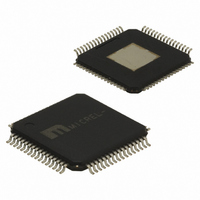
SY89531LHC Micrel Inc, SY89531LHC Datasheet - Page 9

SY89531LHC
Manufacturer Part Number
SY89531LHC
Description
IC SYNTHESIZR LVPECL/HSTL 64TQFP
Manufacturer
Micrel Inc
Series
Precision Edge®r
Type
Clock/Frequency Synthesizerr
Datasheet
1.SY89531LHZ.pdf
(16 pages)
Specifications of SY89531LHC
Pll
Yes
Input
Crystal
Output
HSTL, LVPECL
Number Of Circuits
1
Ratio - Input:output
1:13
Differential - Input:output
No/Yes
Frequency - Max
500MHz
Divider/multiplier
Yes/No
Voltage - Supply
1.6 V ~ 3.6 V
Operating Temperature
0°C ~ 85°C
Mounting Type
Surface Mount
Package / Case
64-TQFP Exposed Pad, 64-eTQFP, 64-HTQFP, 64-VQFP
Frequency-max
500MHz
Lead Free Status / RoHS Status
Contains lead / RoHS non-compliant
Available stocks
Company
Part Number
Manufacturer
Quantity
Price
Micrel, Inc.
precision PLL driven by 14MHz to 18MHz series resonant
crystal. For users who wish to supply a TTL or LVPECL
clock input, please use the SY89536L. The PLL output is
sent to three banks of outputs. Each bank has its own
programmable frequency divider, and the design is optimized
to provide very low skew between banks, and very low
jitter.
PLL Programming and Operation
must be tied LOW, and ExtVCO pins can be left
unconnected.
feedback ratio is selectable via the MSEL divider control
(M3:0 pins). The VCO_SEL pin must be tied low. The
feedback ratio can be changed without powering the chip
down. The PLL output is fed to three banks of outputs:
Bank A, Bank B, and Bank C. Banks A and C each have
two differential LVPECL output pairs. Bank B has nine
differential HSTL output pairs.
can be reprogrammed on the fly. The FSEL_x0:2 (where x
is A, B, or C) pins control the divider value. The FSEL
divider can be programmed in ratios from 2 to 18, and the
outputs of Banks A, B, and C can be synchronized after
programming by pulsing the OUT_SYNC pin HIGH-LOW-
HIGH. Setting a value of 000 for FSEL is an output disable
forcing the Q outputs to be LOW and the /Q outputs to be
HIGH. Doing so will decrease power consumption by
approximately 5mA per bank.
these steps:
1. Refer to the “Suggested Selections for Specific
2. Determine the desired output frequency, such as
3. Choose a crystal frequency between 14MHz and 18MHz.
4. Refer to the “Feedback Divide Select” table and the
5. Make sure that XTAL (the crystal frequency) multiplied
frequencies to satisfy these requirements.
M9999-010808
hbwhelp@micrel.com or (408) 955-1690
FUNCTIONAL DESCRIPTION
Customer Applications” section for common applications,
as well as the formula used to compute the output
frequency.
66MHz.
In this example, we choose 18MHz for the crystal
frequency. This results in an input/output ratio of 66/18.
“Post-Divide Frequency Select” table to find values for
MSEL and FSEL such that MSEL/FSEL equals the same
66/18 ratio. In this example, values of MSEL=44 and
FSEL=12 work.
by MSEL is between 600MHz and 1000MHz.
At the core of the SY89531L clock synthesizer is a
IMPORTANT: If the internal VCO will be used, VCO_SEL
The internal VCO range is 600MHz to 1000MHz, and the
Each bank has a separate frequency divider circuit that
To determine the correct settings for the SY89531L follow
The user may need to experiment with different crystal
9
ExtVCO Input Interface
differential or single-ended input signal within 300mV above
V
the true or complement inputs to ground, but not both. A
logic zero is achieved by connecting the complement input
to ground with the true input floating. For a TTL input, see
“Input Interface for ExtVCO Pins” section, Figures 5a
through 5h.
Input Levels
connected directly to the ExtVCO inputs. Depending on the
actual worst case voltage seen, the minimum input voltage
swing varies.
CC
The flexible ExtVCO inputs are designed to accept any
Do not leave unused ExtVCO inputs floating. Tie either
LVDS, CML and HSTL differential signals may be
and 300mV below ground.
/EXTVCO
EXTVCO
Figure 1. Simplified Input Structure
825
825
R1
R1
990
R2
GND
V
CC
Precision Edge
R2
990
SY89531L
®


