SY89420VJC Micrel Inc, SY89420VJC Datasheet

IC PHASE LOCK LOOP 5/3.3V 28PLCC

SY89420VJC

Manufacturer Part Number
SY89420VJC
Description
IC PHASE LOCK LOOP 5/3.3V 28PLCC
Manufacturer
Micrel Inc
Series
ClockWorks™r
Type
Phase Lock Loop (PLL)r
Datasheet

Specifications of SY89420VJC

Pll
Yes
Input
PECL, TTL
Output
PECL
Number Of Circuits
1
Ratio - Input:output
1:2
Differential - Input:output
Yes/Yes
Frequency - Max
1.12GHz
Divider/multiplier
Yes/No
Voltage - Supply
3.135 V ~ 5.25 V
Operating Temperature
0°C ~ 85°C
Mounting Type
Surface Mount
Package / Case
28-LCC (J-Lead)
Frequency-max
1.12GHz
Number Of Elements
2
Supply Current
200mA
Pll Input Freq (min)
30MHz
Pll Input Freq (max)
560MHz
Operating Supply Voltage (typ)
3.3/5V
Operating Temp Range
0C to 85C
Package Type
PLCC
Output Frequency Range
30 to 1120MHz
Operating Supply Voltage (min)
3.135V
Operating Supply Voltage (max)
5.25V
Operating Temperature Classification
Commercial
Pin Count
28
Lead Free Status / RoHS Status
Contains lead / RoHS non-compliant

Available stocks

Company
Part Number
Manufacturer
Quantity
Price
Part Number:
SY89420VJC
Manufacturer:
Micrel Inc
Quantity:
10 000
Part Number:
SY89420VJC TR
Manufacturer:
Micrel Inc
Quantity:
10 000
FEATURES
3.3V and 5V power supply options
1.12GHz maximum VCO frequency
30MHz to 560MHz reference input operating
frequency
Frequency doubler mode
Low jitter design
PECL differential outputs
PECL and TTL reference voltages available
External loop filter optimizes performance/cost
Available in 28-pin PLCC package
APPLICATIONS
Workstations
Advanced communications
High-end consumer
High-performance computing
PIN CONFIGURATION
FOUTB
FOUTB
FOUTA
FOUTA
V
V
CCOB
CCOA
V
CC
26
27
28
4
2
3
1
25 24 23 22 21 20 19
5
6
TOP VIEW
7
PLCC
J28-1
8
9
10 11
18
17
16
15
14
13
12
5V/3.3V DUAL
PHASE LOCKED LOOP
RINB
RINB
S4B
V
RINA
RINA
V
EE
BB
1
jitter, digital Phase Locked Loops based on Micrel-Synergy's
differential PLL technology. Each of the PLLs (PLLA and
PLLB) is capable of operating in the 30MHz to 560MHz
input reference frequency range independently of the other
and is configurable separately. The PLLs can be configured
to be matched in all regards, or can be configured so that
PLLB is used as a frequency doubler, while PLLA is used
to regenerate the undoubled frequency.
inputs (FINX and FINX), two filter pins (F1X and F2X) and
two differential outputs (FOUTX and FOUTX) are provided
for each of the two PLLs. The reference and feedback
inputs can be used as either differential or single-ended
inputs. In single-ended mode RINX and FINX can be
connected to either V
V
FOUTX to FINX, FINX by means of external circuitry. This
allows the user the flexibility of inserting additional circuitry
off-chip in the feedback paths, such as a divider. Pulldown
resistors are required for the FOUTX and FOUTX pins.
PLL locking and tracking characteristics. Error correction
voltages are generated by the detector if either phase or
frequency deviations occur. The VCO has a frequency
range covering more than a 2:1 ratio from 480MHz to
1120MHz.
dividers for optimum VCO operation, in other words with
the VCO in the center of its range. Additional select pins,
S3B and S4B, are provided for PLLB. When both S3B and
S4B are low, PLLB is identical to PLLA. When S3B is high,
N
frequency doubler option is enabled (P = 2). All Select pins
are TTL compatible.
TH
B
DESCRIPTION
The SY89420V device consists of two identical, low
Two reference inputs (RINX and RINX), two feedback
Feedback for the loops is realized by connecting FOUTX,
Use of a phase-frequency detector results in excellent
Select pins S1X and S2X are used to program the N
can be set to 1, 10, 18, or 20. When S4B is high, the
for normal TTL levels.
BB
for normal 100K PECL levels or
ClockWorks™
Rev.: K
Issue Date: May 2000
SY89420V
Amendment: /0
FINAL

Related parts for SY89420VJC

SY89420VJC Summary of contents

Page 1

FEATURES 3.3V and 5V power supply options 1.12GHz maximum VCO frequency 30MHz to 560MHz reference input operating frequency Frequency doubler mode Low jitter design PECL differential outputs PECL and TTL reference voltages available External loop filter optimizes performance/cost Available in ...

Page 2

Micrel BLOCK DIAGRAM RINA D RINA PHASE-FREQUENCY FINA D FINA RINB D RINB PHASE-FREQUENCY FINB ÷ (1, 2) FINB S4B F1A F2A LOOP FILTER DETECTOR S1B S2B S3B DETECTOR P LOOP FILTER F1B F2B 2 VCO ...

Page 3

Micrel LOOP FILTER COMPONENT SELECTION R F1X C = 1.0 F 10% (X7R dielectric 560 10% PIN NAMES Pin Function F1A Filter Pin 1A F2A Filter Pin 2A RINA Reference Input A RINA Inverted Reference Input A FINA ...

Page 4

Micrel FREQUENCY SELECTION TABLE PLLA S2A S1A PLLB S3B S2B S4B 0 1 ABSOLUTE MAXIMUM RATINGS ...

Page 5

Micrel 5V DC ELECTRICAL CHARACTERISTICS 5. CCOA CCOB Symbol Parameter V Power Supply Voltage CC I Power Supply Current ( Power Supply Current (V CCO 3.3V DC ELECTRICAL CHARACTERISTICS V ...

Page 6

... FOUTA Output Frequency PLLA FOUTB Output Frequency PLLB RINA, B Input Frequency PLLA, B APPLICATION 50MHz Clock SY89429A 16MHz PRODUCT ORDERING CODE Ordering Package Code Type SY89420VJC J28-1 SY89420VJCTR J28-1 5% Min. Typ. — — 300 — 300 — — — — — — ...

Page 7

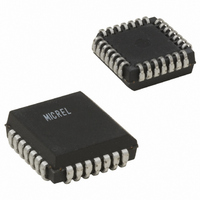
Micrel 28 LEAD PLCC (J28-1) 7 ClockWorks™ SY89420V Rev. 03 ...

Page 8

... TEL This information is believed to be accurate and reliable, however no responsibility is assumed by Micrel for its use nor for any infringement of patents or other rights of third parties resulting from its use. No license is granted by implication or otherwise under any patent or patent right of Micrel Inc (408) 914-7878 http://www ...

Related keywords