NJM567D NJR, NJM567D Datasheet - Page 7

NJM567D
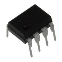
Manufacturer Part Number
NJM567D
Description
IC TONE-DECODER/PH-LCKDLOOP 8DIP
Manufacturer
NJR
Type
Phase Lock Loop (PLL)r
Datasheet
1.NJM567D.pdf
(10 pages)
Specifications of NJM567D
Pll
Yes
Input
Clock
Output
Clock
Number Of Circuits
1
Ratio - Input:output
1:1
Differential - Input:output
No/No
Frequency - Max
500kHz
Divider/multiplier
No/No
Voltage - Supply
4.75 V ~ 9 V
Operating Temperature
-40°C ~ 85°C
Mounting Type
Through Hole
Package / Case
8-DIP
Frequency-max
500kHz
Lead Free Status / RoHS Status
Contains lead / RoHS non-compliant
Available stocks
Company
Part Number
Manufacturer
Quantity
Price
Part Number:
NJM567D
Manufacturer:
JRC
Quantity:
20 000
transient. Thus, maximum operating speed is obtained when C
phase may be such as to initially drive the controlled oscillator away form the incoming frequency rather than toward it.
Under this condition, which is of course unpredictable, the lock-up transient is at its worst and the theoretical minimum
lock-up time is not achievable. We must simply wait for the transient to die out.
frequencies. The minimum rate at which digital information may be detected without information loss due to the turn-on
transient or output chatter is about 10 cycles per bit, corresponding to an information transfer rate of f
used to move the quiescent C
noise and extraneous signals will be increased.
however, will be greatly facilitated if full advantage is taken of the added control possibilities available through the use of
additional external components. In the diagrams given, typical values are suggested where applicable. For best results
the resistors used,except where noted, should have the same temperature coefficient. Ideally, silicon diodes woulds be
low-resistivity types, such as forward-biased transistor base-emitter junctions. However, ordinary low-voltage diodes
should be adequate for most applications.
improve noise and outband signal rejection. This will inevitably slow the response time. If, however, the output stage is
biased closer to the threshold level, the turn-on time can be improved. This is accomplished by drawing additional current
to terminal 1. Under this condition, the 567 will also give an output for Lower-level signals (10mV or lower).
when, to obtain maximum operating speed. C
detection band could cause false outputs under this condition. By desensitizing the output stage, the outband beat notes
do not feed through to the output stage. Since the input level must be somewhat greater when the output stage is made
less sensitive, rejection of third harmonics or in-band harmonics (of lower frequency signals) is also improved.
Ver.2003-12-09
◎ Speed of Operation
◎ Optional Controls (Figure 3)
◎ Sensitivity Adjustment (Figure 3)
Minimum lock-up time is related to the natural frequency of the loop. The lower it is, the longer becomes the turn-on
The following expressions give the values of C
In cases where turn-off time can be sacrificed to achieve fast turn-on, the optional sensitivity adjustment circuit can be
The 567 has been designed so that, for most applications, no external adjustments are required. Certain applications,
When operated as a very narrow band detector (less than 8 precent), both C
By adding current to terminal 1, the output stage is biased further away from the threshold voltage. This is most useful
C
C
2
3
=
=
130
260
f
f
O
O
µ
µ
F
F
3
voltage lower (closer to the threshold voltage). However, sensitivity to beat frequencies,
2
2
and C
and C
Figure 3
3
3
are made very small. Normally, frequencies just outside the
which allow highest operating speeds for various band center
2
is at a minimum. When the signal is frist applied, the
2
and C
3
are made quite large in order to
O
/10 baud.
- 7 -


