MAX9450EHJ+T Maxim Integrated Products, MAX9450EHJ+T Datasheet - Page 6
MAX9450EHJ+T
Manufacturer Part Number
MAX9450EHJ+T
Description
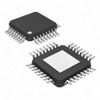
IC CLOCK GENERATOR W/VCXO 32TQFP
Manufacturer
Maxim Integrated Products
Type
Clock Generatorr
Datasheet
1.MAX9451EHJ.pdf
(18 pages)
Specifications of MAX9450EHJ+T
Pll
Yes
Input
LVCMOS, LVDS, LVPECL
Output
LVPECL
Number Of Circuits
1
Ratio - Input:output
2:2
Differential - Input:output
Yes/Yes
Frequency - Max
160MHz
Divider/multiplier
Yes/No
Voltage - Supply
2.4 V ~ 3.6 V
Operating Temperature
-40°C ~ 85°C
Mounting Type
Surface Mount
Package / Case
32-TQFP Exposed Pad, 32-eTQFP, 32-HTQFP, 32-VQFP
Frequency-max
160MHz
Lead Free Status / RoHS Status
Lead free / RoHS Compliant


High-Precision Clock Generators
with Integrated VCXO
6
14, 15
18, 24
19, 20
22, 23
26, 27
29, 30
6, 25
PIN
2, 3
4, 5
7, 8
EP
_______________________________________________________________________________________
10
11
12
13
16
17
21
28
31
32
1
9
S E L0, S E L1
IN0+, IN0- Differential Reference Input Pair. IN0+ and IN0- accept LVPECL, LVDS, and LVCMOS signals.
IN1+, IN1- Differential Reference Input Pair. IN1+ and IN1- accept LVPECL, LVDS, and LVCMOS signals.
AD0, AD1
LP1, LP2
GND/CS
CLK0+
CLK1+
CMON
CLK0-,
CLK1-,
NAME
X1, X2
GNDA
LOCK
V
V
GND
SDA
V
SCL
INT
MR
OE
DDQ
DDA
RJ
EP
DD
Lock Indicator. LOCK goes low when the PLL locks. LOCK is high when the PLL is not locked.
INO_ and IN1_ Select Inputs. Drive SEL0 high to activate IN0; drive SEL1 high to activate IN1. Driving SEL0
and SEL1 low disables the corresponding input. A 165kΩ pullup resistor pulls SEL0 and SEL1 up to V
Digital Power Supply. Connect a 2.4V to 3.6V power supply to V
capacitor.
Reference Input Condition Indicator. A high indicates a failed reference.
Master Reset. Drive MR high to reset all I
Ground and Chip-Select Input. Connect to GND in I
Clock Input. SCL is the clock input in I
Data Input. SDA is the data input in I
I
becomes CS. See Table 3 for the unique addresses list.
Clock Monitor. Drive CMON low to enable the clock monitor. Drive CMON high to disable the clock monitor.
Output Enable Input. Drive OE low to enable the clock outputs. Driving OE high disables the clock outputs,
and the outputs go high impedance. An internal 165kΩ pullup resistor pulls OE up to V
Clock-Output Power Supply. Connect a 2.4V to 3.6V power supply to V
Connect a 1.5V power supply to V
GND.
Differential Clock Output 0. The MAX9450 features LVPECL outputs. The MAX9451 features HSTL outputs
and the MAX9452 features LVDS outputs.
Digital GND
Differential Clock Output 1. The MAX9450 features LVPECL outputs. The MAX9451 features HSTL outputs,
and the MAX9452 features LVDS outputs.
Reference Crystal Input. Connect the reference crystal from X1 to X2.
Anal og P ow er S up p l y. C onnect a 2.4V to 3.6V p ow er sup p l y to V
cap aci tor .
External Loop Filter. Connect an RC circuit between LP1 and LP2. See the External Loop Filter section.
Analog Ground
Charge-Pump Set Current. Connect an external resistor to GND to set the charge-pump current. See
Table 11.
Exposed Paddle. Connect to ground.
2
C Address Selection. Drive AD0 and AD1 high to convert the serial interface from I
DDQ
2
C bus mode and SPI bus mode.
2
C bus mode and SPI bus mode.
for the MAX9451. Connect a 0.1µF bypass capacitor from V
2
C registers to their default state and INT to zero.
FUNCTION
2
C mode. This is the chip-select input in SPI mode.
D D A
DD
. Byp ass V
. Bypass V
DDQ
D D A
for the MAX9450 and MAX9452.
DD
to GN D A w i th a 0.1µF
to GND with a 0.1µF
Pin Description
2
C to SPI. GND/CS
DD
.
DDQ
DD
to
.
Related parts for MAX9450EHJ+T
Image
Part Number
Description
Manufacturer
Datasheet
Request
R

Part Number:
Description:
MAX7528KCWPMaxim Integrated Products [CMOS Dual 8-Bit Buffered Multiplying DACs]
Manufacturer:
Maxim Integrated Products
Datasheet:
Part Number:
Description:
Single +5V, fully integrated, 1.25Gbps laser diode driver.
Manufacturer:
Maxim Integrated Products
Datasheet:
Part Number:
Description:
Single +5V, fully integrated, 155Mbps laser diode driver.
Manufacturer:
Maxim Integrated Products
Datasheet:
Part Number:
Description:
VRD11/VRD10, K8 Rev F 2/3/4-Phase PWM Controllers with Integrated Dual MOSFET Drivers
Manufacturer:
Maxim Integrated Products
Datasheet:
Part Number:
Description:
Highly Integrated Level 2 SMBus Battery Chargers
Manufacturer:
Maxim Integrated Products
Datasheet:
Part Number:
Description:
Current Monitor and Accumulator with Integrated Sense Resistor; ; Temperature Range: -40°C to +85°C
Manufacturer:
Maxim Integrated Products
Part Number:
Description:
TSSOP 14/A�/RS-485 Transceivers with Integrated 100O/120O Termination Resis
Manufacturer:
Maxim Integrated Products
Part Number:
Description:
TSSOP 14/A�/RS-485 Transceivers with Integrated 100O/120O Termination Resis
Manufacturer:
Maxim Integrated Products
Part Number:
Description:
QFN 16/A�/AC-DC and DC-DC Peak-Current-Mode Converters with Integrated Step
Manufacturer:
Maxim Integrated Products
Part Number:
Description:
TDFN/A/65V, 1A, 600KHZ, SYNCHRONOUS STEP-DOWN REGULATOR WITH INTEGRATED SWI
Manufacturer:
Maxim Integrated Products
Part Number:
Description:
Integrated Temperature Controller f
Manufacturer:
Maxim Integrated Products
Part Number:
Description:
SOT23-6/I�/45MHz to 650MHz, Integrated IF VCOs with Differential Output
Manufacturer:
Maxim Integrated Products
Part Number:
Description:
SOT23-6/I�/45MHz to 650MHz, Integrated IF VCOs with Differential Output
Manufacturer:
Maxim Integrated Products
Part Number:
Description:
EVALUATION KIT/2.4GHZ TO 2.5GHZ 802.11G/B RF TRANSCEIVER WITH INTEGRATED PA
Manufacturer:
Maxim Integrated Products
Part Number:
Description:
QFN/E/DUAL PCIE/SATA HIGH SPEED SWITCH WITH INTEGRATED BIAS RESISTOR
Manufacturer:
Maxim Integrated Products
Datasheet: