CS82C84A Intersil, CS82C84A Datasheet
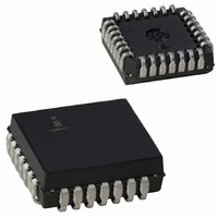
IC CLOCK GEN 5V 25MHZ 20-PLCC

CS82C84A

Manufacturer Part Number
CS82C84A
Description
IC CLOCK GEN 5V 25MHZ 20-PLCC
Manufacturer
Intersil
Type
Clock Generator, Clock Synchronizer, Fanout Distributionr
Datasheet

Specifications of CS82C84A

Pll
No
Input
TTL
Output
TTL
Number Of Circuits
1
Ratio - Input:output
1:3
Differential - Input:output
No/No
Frequency - Max
25MHz
Divider/multiplier
Yes/No
Voltage - Supply
4.5 V ~ 5.5 V
Operating Temperature
0°C ~ 70°C
Mounting Type
Surface Mount
Package / Case
20-PLCC
Frequency-max
25MHz
Lead Free Status / RoHS Status
Contains lead / RoHS non-compliant

Available stocks

Company
Part Number
Manufacturer
Quantity
Price
Part Number:
CS82C84A
Manufacturer:
Intersil
Quantity:
138
Part Number:
CS82C84A
Manufacturer:
HARRIS
Quantity:
50
Part Number:
CS82C84A
Manufacturer:
Intersil
Quantity:
10 000
Part Number:
CS82C84A
Manufacturer:
HAR
Quantity:
2 327
Part Number:
CS82C84A
Manufacturer:
HARRIS
Quantity:
20 000
Part Number:
CS82C84AZ
Manufacturer:
Intersil
Quantity:
10 000
Part Number:
CS82C84AZ96
Manufacturer:
Intersil
Quantity:
10 000
CMOS Clock Generator Driver
The Intersil 82C84A is a high performance CMOS Clock
Generator-driver which is designed to service the requirements
of both CMOS and NMOS microprocessors such as the
80C86, 80C88, 8086 and the 8088. The chip contains a crystal
controlled oscillator, a divide-by-three counter and complete
“Ready” synchronization and reset logic.
Static CMOS circuit design permits operation with an external
frequency source from DC to 25MHz. Crystal controlled
operation to 25MHz is guaranteed with the use of a parallel,
fundamental mode crystal and two small load capacitors.
All inputs (except X1 and RES) are TTL compatible over
temperature and voltage ranges.
Power consumption is a fraction of that of the equivalent
bipolar circuits. This speed-power characteristic of CMOS
permits the designer to custom tailor his system design with
respect to power and/or speed requirements.
Ordering Information
CP82C84A
CP82C84AZ
(See Note)
IP82C84A
CS82C84A
CS82C84AZ
(Note)
CS82C84AZ96
(Note)
IS82C84A
CD82C84A
ID82C84A
MD82C84A/B
8406801VA
MR82C84A/B
84068012A
*Pb-free PDIPs can be used for through hole wave solder processing
only. They are not intended for use in Reflow solder processing
applications.
NOTE: Intersil Pb-free plus anneal products employ special Pb-free
material sets; molding compounds/die attach materials and 100% matte
tin plate termination finish, which are RoHS compliant and compatible
with both SnPb and Pb-free soldering operations. Intersil Pb-free
products are MSL classified at Pb-free peak reflow temperatures that
meet or exceed the Pb-free requirements of IPC/JEDEC J STD-020.
NUMBER
PART
CP82C84A
CP82C84AZ
IP82C84A
CS82C84A
CS82C84AZ
CS82C84AZ
IS82C84A
CD82C84A
ID82C84A
MD82C84A/B
8406801VA
MR82C84A/B
84068012A
MARKING
PART
®
RANGE (°C)
-55 to +125 18 Ld CERDIP F18.3
-55 to +125 18 Ld CERDIP
-55 to +125 20 Pad CLCC J20.A
-55 to +125 20 Pad CLCC
1
-40 to +85
-40 to +85
-40 to +85
0 to +70
0 to +70
0 to +70
0 to +70
0 to +70
0 to +70
TEMP.
Data Sheet
18 Ld PDIP
18 Ld PDIP*
(Pb-free)
18 Ld PDIP
20 Ld PLCC
20 Ld PLCC
(Pb-free)
20 Ld PLCC
Tape and Reel
(Pb-free)
20 Ld PLCC
18 Ld CERDIP F18.3
18 Ld CERDIP F18.3
SMD#
SMD#
PACKAGE
1-888-INTERSIL or 1-888-468-3774
E18.3
E18.3
E18.3
N20.35
N20.35
N20.35
N20.35
F18.3
J20.A
DWG. #
PKG.
CAUTION: These devices are sensitive to electrostatic discharge; follow proper IC Handling Procedures.
Features
• Generates the System Clock For CMOS or NMOS
• Up to 25MHz Operation
• Uses a Parallel Mode Crystal Circuit or External
• Provides Ready Synchronization
• Generates System Reset Output From Schmitt Trigger
• TTL Compatible Inputs/Outputs
• Very Low Power Consumption
• Single 5V Power Supply
• Operating Temperature Ranges
• Pb-Free Plus Anneal Available (RoHS Compliant)
Pinouts
Microprocessors
Frequency Source
Input
- C82C84A . . . . . . . . . . . . . . . . . . . . . . . . . 0°C to +70°C
- I82C84A . . . . . . . . . . . . . . . . . . . . . . . . . -40°C to +85°C
- M82C84A . . . . . . . . . . . . . . . . . . . . . . . -55°C to +125°C
December 6, 2005
All other trademarks mentioned are the property of their respective owners.
READY
|
RDY1
RDY2
AEN2
Copyright Intersil Americas Inc. 1997, 2002, 2005. All Rights Reserved
Intersil (and design) is a registered trademark of Intersil Americas Inc.
CSYNC
READY
NC
PCLK
AEN1
RDY1
RDY2
AEN2
GND
CLK
4
5
6
7
8
82C84A (PDIP, CERDIP)
82C84A (PLCC, CLCC)
1
2
3
4
5
6
7
8
9
3
9
10
TOP VIEW
TOP VIEW
2
11
1
12
20
19
13
18
17
16
15
14
13
12
11
10
18
17
16
15
14
V
X1
X2
ASYNC
EFI
F/C
OSC
RES
RESET
CC
82C84A
X2
ASYNC
EFI
F/C
NC
FN2974.3

Related parts for CS82C84A

CS82C84A Summary of contents

Page 1

... RANGE (°C) CP82C84A CP82C84A 0 to +70 CP82C84AZ CP82C84AZ 0 to +70 (See Note) IP82C84A IP82C84A -40 to +85 CS82C84A CS82C84A 0 to +70 CS82C84AZ CS82C84AZ 0 to +70 (Note) CS82C84AZ96 CS82C84AZ 0 to +70 (Note) IS82C84A IS82C84A -40 to +85 CD82C84A CD82C84A 0 to +70 ID82C84A ID82C84A -40 to +85 MD82C84A/B MD82C84A/B -55 to +125 18 Ld CERDIP F18.3 8406801VA 8406801VA ...

Page 2

Functional Diagram 11 RES F/C 14 EF1 1 CSYNC 4 RDY1 3 AEN1 6 RDY2 7 AEN2 15 ASYNC 2 82C84A 82C84A XTAL OSCILLATOR SYNC FF1 CONTROL PIN LOGICAL 1 F/C External ...

Page 3

Pin Description SYMBOL NUMBER TYPE AEN1 AEN2 RDY1 RDY2 ASYNC 15 I READY 5 O X1 EFI 14 I CLK 8 O PCLK 2 O OSC ...

Page 4

Functional Description Oscillator The oscillator circuit of the 82C84A is designed primarily for use with an external parallel resonant, fundamental mode crystal from which the basic operating frequency is derived. The crystal frequency should be selected at three times the ...

Page 5

CLOCK SYNCHRONIZE EFI NOTE: If EFI input is used, then crystal input X1 must be tied to V then EFI should be tied GND 82C84A 82C84A > > or GND and ...

Page 6

Absolute Maximum Ratings Supply Voltage ...

Page 7

AC Electrical Specifications SYMBOL TIMING REQUIREMENTS TEHEL External Frequency HIGH Time (1) TELEH External Frequency LOW Time (2) TELEL EFI Period (3) XTAL Frequency TR2VCL RDY1, RDY2 Active Setup to CLK (4) ...

Page 8

Timing Waveforms (3) NAME I/O EFI I OSC O CLK O PCLK O (13) tEHYL CSYNC I (14) tYHYL I RES RESET O NOTE: All timing measurements are made at 1.5V, unless otherwise noted. FIGURE 2. WAVEFORMS FOR CLOCKS AND ...

Page 9

Test Load Circuits NOTES =100pF for CLK output 50pF for all outputs except CLK Includes probe and jig capacitance CLK F/C CSYNC V CC AEN1 ...

Page 10

Burn-In Circuits GND GND GND V CC OPEN NOTES: = 5.5V ±0.5V, GND = 0V 4.5V ±10 ...

Page 11

... Accordingly, the reader is cautioned to verify that data sheets are current before placing orders. Information furnished by Intersil is believed to be accurate and reliable. However, no responsibility is assumed by Intersil or its subsidiaries for its use; nor for any infringements of patents or other rights of third parties which may result from its use ...

Related keywords