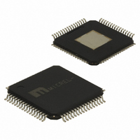
SY89535LHZ Micrel Inc, SY89535LHZ Datasheet - Page 8

SY89535LHZ
Manufacturer Part Number
SY89535LHZ
Description
IC SYNTHESIZR LVPECL/LVDS 64TQFP
Manufacturer
Micrel Inc
Series
Precision Edge®r
Type
Clock/Frequency Synthesizerr
Datasheet
1.SY89534LHZ.pdf
(15 pages)
Specifications of SY89535LHZ
Pll
Yes with Bypass
Input
CMOS, HSTL, LVDS, LVPECL, LVTTL, SSTL
Output
LVDS, LVPECL
Number Of Circuits
1
Ratio - Input:output
1:13
Differential - Input:output
Yes/Yes
Frequency - Max
500MHz
Divider/multiplier
Yes/No
Voltage - Supply
3 V ~ 3.6 V
Operating Temperature
0°C ~ 85°C
Mounting Type
Surface Mount
Package / Case
64-TQFP Exposed Pad, 64-eTQFP, 64-HTQFP, 64-VQFP
Frequency-max
500MHz
Lead Free Status / RoHS Status
Lead free / RoHS Compliant
Available stocks
Company
Part Number
Manufacturer
Quantity
Price
Micrel, Inc.
precision PLL driven by a differential or single-ended reference
input. For users who wish to supply a crystal input, please use
the SY89532L or SY89533L. The PLL output is sent to three
banks of outputs. Each bank has its own programmable
frequency divider, and the design is optimized to provide very
low skew between banks, and very low jitter.
PLL Programming and Operation
feedback ratio is selectable via the MSEL divider control (M3:0
pins). The feedback ratio can be changed without powering
the chip down. The PLL output is fed to three banks of outputs:
Bank A, Bank B, and Bank C. Banks A and C each have two
differential LVPECL output pairs. Bank B has nine differential
output pairs. On the SY89534L, Bank B is LVPECL. On the
SY89535L, Bank B is LVDS.
be reprogrammed on the fly. The FSEL_x0:2 (where x is A, B,
or C) pins control the divider value. The FSEL divider can be
programmed in ratios from 2 to 18, and the outputs of Banks
A, B, and C can be synchronized after programming by
pulsing the OUT_SYNC pin HIGH-LOW-HIGH.
these steps:
Applications” section for common applications, as well as the
formula used to compute the output frequency.
66MHz.
and 20MHz. The user can also choose a higher input frequency,
and use the PSEL pre-divider to divide it down to the 14MHz
to 20MHz range. In this example, we choose 18MHz for the
reference input frequency. This results in an input/output ratio
of 66/18.
“Post-Divide Frequency Select Table” to find values for MSEL
and FSEL such that MSEL/FSEL equals the same 66/18 ratio.
In this example, values of MSEL=44 and FSEL=12 work.
600MHz and 1000MHz.
input frequencies to satisfy these requirements.
M9999-110308
hbwhelp@micrel.com or (408) 955-1690
FUNCTIONAL DESCRIPTION
At the core of the SY89534/35L clock synthesizer is a
The internal VCO range is 600MHz to 1000MHz, and the
Each bank has a separate frequency divider circuit that can
To determine the correct settings for SY89534/35L follow
1. Refer to the “Suggested Selections for Specific Customer
2. Determine the desired output frequency, such as
3. Choose a reference input frequency between 14MHz
4. Refer to the “Feedback Divide Select Table” and the
5. Make sure that REFCLK
The user may need to experiment with different REFCLK
Figure 1. External Loop Filter Connection
Loop
Filter
330
470pF
0.2 F
PSEL
Reference
Loop
MSEL is between
8
External Loop Filter Considerations
allows the user to tailor the PLL’s behavior to their application
and operating environment. We recommend using ceramic
capacitors with NPO or X7R dielectric, as they have very low
effective series resistance. For applications that require ultra-
low cycle-to-cycle jitter, use the components shown in Figure
1. The PLL loop bandwidth is a function of feedback divider
ratio, and the external loop filter allows the user to compensate.
For instance, the PLL’s loop bandwidth can be decreased by
using a smaller resistor in the loop filter. This results in less
noise from the PLL input, but potentially more noise from the
VCO. Refer to “AC Electrical Characteristics” for target PLL
loop bandwidth. The designer should take care to keep the
loop filter components on the same side of the board and as
close as possible to the SY89534/35L’s LOOP_REF and
LOOP_FILTER pins. To insure minimal noise pick-up on the
loop filter, it is desirable to cut away the ground plane directly
underneath the loop filter component pads and traces.
However, the benefit may not be significant in all applications
and one must be careful to not alter the characteristic
impedance of nearby traces.
Power Supply Filtering Techniques
filtering is very important. At a minimum, V
and all V
to the power supply plane, and separate bypass capacitors
should be used for each pin. To achieve optimal jitter
performance, each power supply pin should use separate
instances of the circuit shown in Figure 2.
The SY89534/35L features an external PLL loop filter that
As with any high-speed integrated circuit, power supply
CCO
*For V
use ferrite bead = 200mA, 0.45 DC,
Murata P/N BLM21A1025
*For V
Murata, P/N BLM31P005
*Component size: 0805
Figure 2. Power Supply Filtering
pins should be individually connected using a via
“Power Supply”
CC_
CC_OUT
side
22 F
Analog,V
use ferrite bead = 3A, 0.025 DC,
Ferrite Bead*
CC_TTL,
V
CC1,
1 F
“Device”
0.01 F
CC
side
Precision Edge
A, V
Pins
V
SY89534/35L
CC
CC
_Logic,
®


