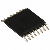
CY22150FZXI Cypress Semiconductor Corp, CY22150FZXI Datasheet - Page 3

CY22150FZXI
Manufacturer Part Number
CY22150FZXI
Description
IC CLOCK GEN PROG 16-TSSOP
Manufacturer
Cypress Semiconductor Corp
Type
Clock Generator, Fanout Distributionr
Specifications of CY22150FZXI
Number Of Circuits
1
Package / Case
16-TSSOP
Pll
Yes
Input
Crystal
Output
Clock
Ratio - Input:output
1:6
Differential - Input:output
No/No
Frequency - Max
166.6MHz
Divider/multiplier
Yes/No
Voltage - Supply
2.375 V ~ 3.465 V
Operating Temperature
-40°C ~ 85°C
Mounting Type
Surface Mount
Frequency-max
167MHz
Maximum Input Frequency
133 MHz
Minimum Input Frequency
1 MHz
Output Frequency Range
0.08 MHz to 166.6 MHz
Supply Voltage (max)
3.465 V
Supply Voltage (min)
3.135 V
Maximum Operating Temperature
+ 85 C
Minimum Operating Temperature
- 40 C
Mounting Style
SMD/SMT
Operating Supply Voltage
3.3 V
Frequency
166.6MHz
No. Of Outputs
6
No. Of Multipliers / Dividers
2
Supply Current
45mA
Supply Voltage Range
2.375V To 2.625V, 3.135V To 3.465V
Digital Ic Case Style
TSSOP
No. Of Pins
16
Rohs Compliant
Yes
Lead Free Status / RoHS Status
Lead free / RoHS Compliant
For Use With
CY30700 - KIT PROG FOR CY22150428-1918 - KIT DEV FTG PROGRAMMING KIT428-1452 - SOCKET ADAPTER FOR CY22050
Lead Free Status / Rohs Status
Lead free / RoHS Compliant
Other names
428-2177-5
CY22150FZXI
CY22150FZXI
Available stocks
Company
Part Number
Manufacturer
Quantity
Price
Part Number:
CY22150FZXI
Manufacturer:
CIRRUS
Quantity:
20 000
Frequency Calculation and Register Definitions
The CY22150 is an extremely flexible clock generator with four
basic variables that are used to determine the final output
frequency. They are the input reference frequency (REF), the
internally calculated P and Q dividers, and the post divider, which
can be a fixed or calculated value. There are three formulas to
determine the final output frequency of a CY22150 based
design:
■
■
■
Document #: 38-07104 Rev. *I
CLK = ((REF * P)/Q)/Post Divider
CLK = REF/Post Divider
CLK = REF.
REF
DIV1N [OCH]
DIV1SRC [OCH]
DIV2SRC [47H]
DIV2N [47H]
CLKOE [09H]
(Q+2)
[42H]
Qtotal
PFD
Figure 2. Basic Block Diagram of CY22150 PLL
[40H], [41H], [42H]
(2(PB+4)+PO)
Ptotal
VCO
The basic PLL block diagram is shown in
six clock outputs on the CY22150 has a total of seven output
options available to it. There are six post divider options
available: /2 (two of these), /3, /4, /DIV1N and /DIV2N. DIV1N
and DIV2N are independently calculated and are applied to
individual output groups. The post divider options can be applied
to the calculated VCO frequency ((REF*P)/Q) or to the REF
directly.
In addition to the six post divider output options, the seventh
option bypasses the PLL and passes the REF directly to the
crosspoint switch matrix.
1
0
1
0
Divider Bank 1
Divider Bank 2
/DIV1N
/DIV2N
/4
/2
/2
/3
Switch Matrix
Crosspoint
CLKSRC
[44H,45H]
[45H,46H]
[45H]
[44H]
[44H]
[45H]
Figure
CY22150
2. Each of the
Page 3 of 16
LCLK1
LCLK2
LCLK3
LCLK4
CLK5
CLK6
[+] Feedback


