AD809BR-REEL7 Analog Devices Inc, AD809BR-REEL7 Datasheet
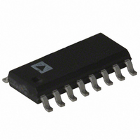
IC SYNTH FREQ 155.52MHZ 16-SOIC

AD809BR-REEL7

Manufacturer Part Number
AD809BR-REEL7
Description
IC SYNTH FREQ 155.52MHZ 16-SOIC
Manufacturer
Analog Devices Inc
Type
Clock/Frequency Synthesizerr
Datasheet

Specifications of AD809BR-REEL7

Rohs Status
RoHS non-compliant
Pll
No
Input
CMOS, ECL, PECL, TTL
Output
ECL, PECL
Number Of Circuits
1
Ratio - Input:output
2:1
Differential - Input:output
Yes/Yes
Frequency - Max
155.52MHz
Divider/multiplier
No/No
Voltage - Supply
4.5 V ~ 5.5 V
Operating Temperature
-40°C ~ 85°C
Mounting Type
Surface Mount
Package / Case
16-SOIC (3.9mm Width)
Frequency-max
155MHz
a
PRODUCT DESCRIPTION
The AD809 provides a 155.52 MHz ECL/PECL output clock from
either a 19.44 MHz or a 9.72 MHz TTL/CMOS/ECL/PECL refer-
ence frequency. The AD809 functionality supports a distributed
timing architecture, allowing a backplane or PCB 19.44 MHz or
9.72 MHz timing reference signal to be distributed to multiple
REV. A
Information furnished by Analog Devices is believed to be accurate and
reliable. However, no responsibility is assumed by Analog Devices for its
use, nor for any infringements of patents or other rights of third parties
which may result from its use. No license is granted by implication or
otherwise under any patent or patent rights of Analog Devices.
FEATURES
Frequency Synthesis to 155.52 MHz
19.44 MHz or 9.72 MHz Input
Reference Signal Select Mux
Single Supply Operation: +5 V or –5.2 V
Output Jitter: 2.0 Degrees RMS
Low Power: 90 mW
10 KH ECL/PECL Compatible Output
10 KH ECL/PECL/TTL/CMOS Compatible Input
Package: 16-Pin Narrow 150 Mil SOIC
(19.44MHz
(155MHz)
9.72MHz) CLKINN
OR
TTL/CMOSIN
PECLINN
PECLIN
CLKIN
MUX
12
10
13
15
2
1
FUNCTIONAL BLOCK DIAGRAM
SELECT
AUTO
AD809
155.52 MHz Frequency Synthesizer
PFD
155.52 Mbps ports. The AD809 can be applied to create the trans-
mit bit clock for one or more ports.
An input signal multiplexer supports loop-timed applications
where a 155.52 MHz transmit bit clock is recovered from the
155.52 Mbps received data.
The low jitter VCO, low power and wide operating temperature
range make the device suitable for generating a 155.52 MHz bit
clock for SONET/SDH/Fiber in the Loop systems.
The device has a low cost, on-chip VCO that locks to either
8 or 16 the frequency at the 19.44 MHz or 9.72 MHz input.
No external components are needed for frequency synthesis; how-
ever, the user can adjust loop dynamics through selection of a
damping factor capacitor whose value determines loop damping.
The AD809 design guarantees that the clock output frequency
will drift low (by roughly 20%) in the absence of a signal at the
input.
The AD809 consumes 90 mW and operates from a single power
supply at either +5 V or –5.2 V.
One Technology Way, P.O. Box 9106, Norwood, MA 02062-9106, U.S.A.
Tel: 617/329-4700
Fax: 617/326-8703
CF1 CF2
FILTER
7
LOOP
BW
ADJUST
8
MUX
DIVIDE BY 8/16
AUTO SELECT
VCO
World Wide Web Site: http://www.analog.com
5
4
CLKOUT
CLKOUTN
(155MHz
PECL
OUTPUT)
© Analog Devices, Inc., 1997
AD809

Related parts for AD809BR-REEL7

AD809BR-REEL7 Summary of contents

Page 1

FEATURES Frequency Synthesis to 155.52 MHz 19.44 MHz or 9.72 MHz Input Reference Signal Select Mux Single Supply Operation –5.2 V Output Jitter: 2.0 Degrees RMS Low Power ECL/PECL Compatible Output 10 ...

Page 2

... Exposure to absolute maximum rating conditions for extended periods may affect device reliability. Thermal Characteristics: 16-Pin Narrow Body SOIC Package: = 110 C/W. JA Model AD809BR AD809BR-REEL7 ( MIN ...

Page 3

PIN DESCRIPTIONS Pin No. Mnemonic Description 1 PECLINN Differential 155 MHz Input 2 PECLIN Differential 155 MHz Input 3 V Digital V for PECL Outputs CC2 CC 4 CLKOUTN Differential 155 MHz Output 5 CLKOUT Differential 155 MHz Output 6 ...

Page 4

AD809 DEFINITION OF TERMS Maximum, Minimum and Typical Specifications Specifications for every parameter are derived from statistical analyses of data taken on multiple devices from multiple wafer lots. Typical specifications are the mean of the distribution of the data for ...

Page 5

USING THE AD809 Ground Planes Use of one ground plane for connections to both analog and digital grounds is recommended. Power Supply Connections Use capacitor between V and ground is recom- CC mended. Care should be ...

Page 6

AD809 Figure 6. Evaluation Board: Component Side Figure 7. Evaluation Board: Solder Side –6– REV. A ...

Page 7

REV. A Figure 8. Evaluation Board: INT2 –7– AD809 ...

Page 8

AD809 PIN 1 0.0098 (0.25) 0.0040 (0.10) OUTLINE DIMENSIONS Dimensions shown in inches and (mm). 16-Lead Small Outline IC Package (R-16A 0.1574 (4.00) 0.1497 (3.80) 0.2440 (6.20 0.2284 (5.80) 0.3937 (10.00) 0.3859 (9.80) 0.0688 (1.75) 0.0532 ...

Related keywords