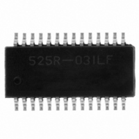
ICS525R-03ILFT IDT, Integrated Device Technology Inc, ICS525R-03ILFT Datasheet - Page 4

ICS525R-03ILFT
Manufacturer Part Number
ICS525R-03ILFT
Description
IC CLOCK USER CONFIG 28-SSOP
Manufacturer
IDT, Integrated Device Technology Inc
Series
OSCaR™r
Type
Clock Generator, Fanout Distributionr
Datasheet
1.ICS525R-03ILFT.pdf
(8 pages)
Specifications of ICS525R-03ILFT
Pll
Yes
Input
PECL
Output
CMOS
Number Of Circuits
1
Ratio - Input:output
1:2
Differential - Input:output
Yes/No
Frequency - Max
250MHz
Divider/multiplier
Yes/No
Voltage - Supply
3 V ~ 5.5 V
Operating Temperature
-40°C ~ 85°C
Mounting Type
Surface Mount
Package / Case
28-SSOP
Frequency-max
250MHz
Lead Free Status / RoHS Status
Lead free / RoHS Compliant
Other names
525R-03ILFT
800-1802-2
800-1802-2
IDT® PECL INPUT OSCAR™ USER CONFIGURABLE CLOCK
ICS525-03
PECL INPUT OSCAR™ USER CONFIGURABLE CLOCK
External Components/Crystal
Selection
Decoupling Capacitors
The ICS525-03 requries two 0.01µF decoupling
capacitors to be connected between VDD and GND,
one on each side of the chip. The capacitor must be
connected close to the device to minimize lead
inductance. No external power supply filtering is
required for this device.
External Resistors
If PECL outputs are desired, RES should be tied to VDD
with a 1.1 k resistor. Each output needs a resistive
network of 62 and 270 per the block diagram on page
1. Application note MAN09 gives more information
about resistor selection.
Determining (setting) the Output Frequency
Users have full control in setting the desired output
frequency over the range shown in the table on page 2.
To replace a standard oscillator, users should connect
the divider select input pins directly to ground (or VDD,
although this is not required because of internal
pull-ups) during Printed Circuit Board layout. The
ICS525-03 will automatically produce the correct clock
when all components are soldered. It is also possible to
connect the inputs to parallel I/O ports to switch
frequencies. By choosing divides carefully, the number
of inputs which need to be changed can be minimized.
Observe the restrictions on allowed values of VDW and
RDW.
The output of the ICS525-03 can be determined by the
following simple equation:
Where:
Reference Divider Word (RDW) = 0 to 127
VCO Divider Word (VDW) = 0 to 511
Output Divider (OD) = values on page 2
CLK
Frequency
=
Input Frequency
P
x
-------------------------------------------- -
RDW
VDW
+
2
+
8
OD
4
Pre-divide (P) = values on page 2 under RES Value
Table
Also, the following operating ranges should be
observed:
(See table on page 2 for full details of maximum output)
The dividers are expressed as integers, so that if a
66.66 MHz PECL output is desired from a 14.31818
PECL input, the Reference Divider Word (RDW) should
be 59 and the VCO Divider Word (VDW) should be 276,
with an Output Divider (OD) of 1. To select PECL
outputs, the RES pin should be tied to VDD with a 1.1k
resistor.
In this example, R6:R0 is 100010100, and S2:S0 is 110.
Since all of these inputs have pull-up reistors, it is only
necessary to ground the zero pins, namely V7, V6, V5,
V3, V1, V0, R6, R2 and S0.
To determine the best combination of VCO, reference,
and output divide, use the ICS525 Calculator on our
web site. The online form is easy to use and quickly
shows you up to three options for these settings.
Alternately, you may send an e-mail to
cmd-support@idt.com.
10 MHz < Input frequency x
200 kHz < Input Frequency
(RDW+2)
(VDW+8)
(RDW+2)
<350 MHz at 5.0 V or
<250 MHz at 3.3 V
ICS525-03
PECL MULTIPLIER
REV L 010311


