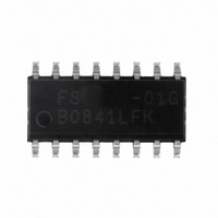
FS6370-01G-XTD ON Semiconductor, FS6370-01G-XTD Datasheet - Page 26

FS6370-01G-XTD
Manufacturer Part Number
FS6370-01G-XTD
Description
IC CLOCK GEN 3-PLL EEPROM 16SOIC
Manufacturer
ON Semiconductor
Type
PLL Clock Generatorr
Datasheet
1.FS6370-01G-XTD.pdf
(28 pages)
Specifications of FS6370-01G-XTD
Pll
Yes
Input
Crystal
Output
CMOS
Number Of Circuits
1
Ratio - Input:output
1:4
Differential - Input:output
No/No
Frequency - Max
230MHz
Divider/multiplier
Yes/No
Voltage - Supply
3 V ~ 5.5 V
Operating Temperature
0°C ~ 70°C
Mounting Type
Surface Mount
Package / Case
16-SOIC (3.9mm Width)
Frequency-max
230MHz
Mounting Style
SMD/SMT
Max Input Freq
230 MHz
Max Output Freq
27 MHz
Number Of Outputs
1
Operating Supply Voltage
5 V to 3.3 V
Operating Temperature Range
0 C to + 70 C
Supply Current
43 mA
Lead Free Status / RoHS Status
Lead free / RoHS Compliant
Other names
766-1025
Available stocks
Company
Part Number
Manufacturer
Quantity
Price
Company:
Part Number:
FS6370-01G-XTD
Manufacturer:
ON Semiconductor
Quantity:
38
FS6370
13.3.1. Example Programming
Type a value for the crystal resonator frequency in MHz in the reference crystal box. This frequency provides the basis for all of the PLL
calculations that follow.
Next, click on the PLL A box. A pop-up screen similar to Figure 15 should appear. Type in a desired output clock frequency in MHz, set
the operating voltage (3.3 V or 5 V), and the desired maximum output frequency error. Pressing calculate solutions generates several
possible divider and VCO-speed combinations.
Figure 15: PLL Screen
For a 100 MHz output, the VCO should ideally operate at a higher frequency, and the reference and feedback dividers should be as
small as possible. In this example, highlight solution #7. Notice the VCO operates at 200MHz with a post divider of 2 to obtain an
optimal 50 percent duty cycle.
Now choose which mux and post divider to use (that is, choose an output pin for the 100 MHz output). Selecting A places the PostDiv
value in solution #7 into post divider A and switches mux A to take the output of PLL A.
The PLL screen should disappear, and now the value in the PLL A box is the new VCO frequency chosen in solution #7. Note that mux
A has been switched to PLL A and the post divider A has the chosen 100MHz output displayed.
Repeat the steps for PLL B.
PLL C supports two different output frequencies depending on the setting of the SEL_CD pin. Both mux C and mux D are also affected
by the logic level on the SEL_CD pin, as are the post dividers C and D (see Section 4.2 for more detail).
Rev. 3 | Page 26 of 28 | www.onsemi.com


