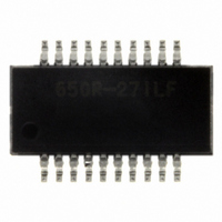
ICS650R-27ILFT IDT, Integrated Device Technology Inc, ICS650R-27ILFT Datasheet - Page 2

ICS650R-27ILFT
Manufacturer Part Number
ICS650R-27ILFT
Description
IC CLOCK SYNTHESIZER 20-SSOP
Manufacturer
IDT, Integrated Device Technology Inc
Type
Clock/Frequency Synthesizerr
Datasheet
1.ICS650R-27I.pdf
(7 pages)
Specifications of ICS650R-27ILFT
Pll
Yes
Input
Clock, Crystal
Output
CMOS
Number Of Circuits
1
Ratio - Input:output
1:7
Differential - Input:output
No/No
Frequency - Max
133.33MHz
Divider/multiplier
Yes/No
Voltage - Supply
3 V ~ 3.6 V
Operating Temperature
-40°C ~ 85°C
Mounting Type
Surface Mount
Package / Case
20-SSOP
Frequency-max
133MHz
Lead Free Status / RoHS Status
Lead free / RoHS Compliant
Other names
650R-27ILFT
800-1813-2
800-1813-2
Pin Assignment
Pin Descriptions
IDT™ / ICS™ NETWORKING CLOCK SOURCE
ICS650-27
NETWORKING CLOCK SOURCE
Number
Pin
10
11
12
13
14
15
16
17
18
19
20
1
2
3
4
5
6
7
8
9
X1/ICLK
CLKC1
CLKC2
CLKB2
CLKB1
ASC0
ASC1
GND
VDD
X2
REFOUT
X1/ICLK
Name
CLKC1
CLKC2
CLKB2
CLKB1
CLKA2
CLKA1
ACS0
ACS1
BCS0
BCS1
GND
GND
VDD
CCS
VDD
Pin
DC
OE
X2
20-pin (150 mil) SSOP
1
2
3
4
5
6
7
8
9
10
Output
Output
Output
Output
Output
Output
Output
Type
Power
Power
Power
Power
Input
Input
Input
Input
Input
Input
Input
Input
Pin
-
20
19
18
17
16
15
14
13
12
11
A clock select 0. Selects outputs on CLKA1 and CLKA2 per table on page 3.
Crystal connection. Connect to a fundamental crystal or leave unconnected for a clock
input.
Crystal connection. Connect to a fundamental crystal or clock input.
Connect to +3.3 V or 5 V. Must be the same as pin 16.
A clock select 1. Selects outputs on CLKA1 and CLKA2 per table on page 3. Internal
pull-up.
Connect to ground.
Output Clock C1. Depends on setting of CCS per table on page 3.
Output Clock C2. Depends on setting of CCS per table on page 3. Same as CLKC1.
Output Clock B2. Depends on setting of BCS1, 0 per table on page 3.
Output Clock B1. Depends on setting of BCS1, 0 per table on page 3.
Clock C select pin. Selects outputs on CLKC1 and CLKC2 per table on page 3.
Don’t connect. Do not connect anything to this pin.
Output Clock A2. Depends on setting of ACS1, 0 per table on page 3.
Connect to ground.
Output enable. Tri-states all outputs when low. Internal pull-up.
Connect to +3.3 V or 5 V. Must be the same as pin 4.
Output Clock A1. Depends on setting of ACS1, 0 per table on page 3.
Buffered reference clock output. Same frequency as crystal or clock input.
B clock select 0. Selects outputs on CLKB1 and CLKB2 per table on page 3.
B clock select 1. Selects outputs on CLKB1 and CLKB2 per table on page 3. Internal
pull-up.
BCS1
BCS0
REFOUT
CLKA1
VDD
OE
GND
CLKA2
DC
CCS
2
Pin Description
CLOCK SYNTHESIZER
ICS650-27
REV F 051310


