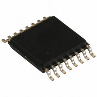
CY22394FXI Cypress Semiconductor Corp, CY22394FXI Datasheet

CY22394FXI
Specifications of CY22394FXI
CY22394FXI
Available stocks
Related parts for CY22394FXI
CY22394FXI Summary of contents
Page 1
... Advanced Features • Serial-programmable • Configurable output buffer • Digital VCXO • High-frequency LVPECL output (CY22394 only) • 3.3/2.5V outputs (CY22395 only) Cypress Semiconductor Corporation Document #: 38-07186 Rev. *B Three-PLL Serial-Programmable Flash-Programmable Clock Generator Benefits • Generates up to three unique frequencies six outputs from an external source. • ...
Page 2
Selector Guide Part Number Outputs Input Frequency Range CY22393FC 6 CMOS 8 MHz–30 MHz (external crystal) 1 MHz–166 MHz (reference clock) CY22393FI 6 CMOS 8 MHz–30 MHz (external crystal) 1 MHz–150 MHz (reference clock) CY22394FC 1 PECL/ 8 MHz–30 MHz ...
Page 3
Logic Block Diagram — CY22395 XTALIN OSC. XTALOUT CONFIGURATION FLASH SHUTDOWN/OE SCLK SDAT S2/SUSPEND LCLKA, LCLKB, LCLKD, LCLKE referenced to LVDD Pin Configurations CY22393 16-pin TSSOP CLKC 1 SHUTDOWN/ S2/SUSPEND AGND AV DD ...
Page 4
Pin Definitions (continued) Pin Number Pin Number Name CY22393 CY22394 CLKA or LCLKA 10 GND/LGND 11 SDAT (S0) 12 SCLK (S1 S2/ 15 SUSPEND SHUTDOWN Operation The CY22393, CY22394, and CY22395 are a family ...
Page 5
Be aware that adjusting the frequency of the reference will affect all frequencies on all PLLs in a similar manner since all frequencies are derived from the single reference. Output Configuration Under normal operation there are four internal frequency sources ...
Page 6
Memory Bitmap Definitions Clk{A–D}_Div[6:0] Each of the four main output clocks (CLKA–CLKD) features a 7-bit linear output divider. Any divider setting may be used between 1 and 127 by programming the value of the desired divider into this register. Odd ...
Page 7
OscCap[5:0] This controls the internal capacitive load of the oscillator. The approximate effective crystal load capacitance is 6pF OscCap = + LOAD Set to zero for external reference clock. OscDrv[1:0] These bits control the crystal oscillator gain setting. ...
Page 8
S2 Addr (1, 4CH 100 4DH 4EH DivSel PLL1_En 4FH 101 50H 51H DivSel PLL1_En 52H 110 53H 54H DivSel PLL1_En 55H 111 56H 57H DivSel PLL1_En Serial Programming Interface (SPI) Protocol and Timing The CY22393,CY22394 and CY22395 ...
Page 9
Read Operations Read operations are initiated the same way as Write opera- tions except that the R/W bit of the slave address is set to ‘1’ (HIGH). There are three basic read operations: current address read, random read, and sequential ...
Page 10
Bit SDAT Write 1 Bit Slave ACK R Multiple 7-bit 8-bit Contiguous Device Register Registers Address Address (XXH) Start Signal 1 Bit SDAT Read 1 Bit Slave ACK R Current 7-bit 8-bit Device Register Address ...
Page 11
SDAT + START DA6 DA5 DA0 R/W + SCLK Figure 5. Frame Format (Device Address, R/W, Register Address, Register Data) Serial Programming Interface Timing Specifications Parameter f Frequency of SCLK SCLK Start mode time from SDA LOW to SCL LOW ...
Page 12
Maximum Ratings (Above which the useful life may be impaired. For user guide- lines, not tested.) Supply Voltage ............................................... –0.5V to +7.0V DC Input Voltage............................ –0. (AV Storage Temperature .................................. –65°C to +125°C Operating Conditions [2] Parameter Description ...
Page 13
Switching Characteristics Parameter Description [4, 6] 1/t Output Frequency 1 [ Output Duty Cycle 2 t Rising Edge Slew 3 [4] Rate t Falling Edge Slew 4 [4] Rate t Output three-state 5 [4] Timing [4, 8] ...
Page 14
Output Three State Timing ALL THREE-STATE OUTPUTS CLK Output Jitter CLK OUTPUT P+/P– Crossing Point and Jitter CPU Frequency Change SELECT OLD SELECT F old CPU Test Circuit AV DD ...
Page 15
... TSSOP CY22394ZXI-XXXT 16-Pin TSSOP - Tape and Reel CY22394FXC 16-Pin TSSOP CY22394FXCT 16-Pin TSSOP- Tape and Reel CY22394FXI 16-Pin TSSOP CY22394FXIT 16-Pin TSSOP - Tape and Reel CY22395ZXC-XXX 16-Pin TSSOP CY22395ZXC-XXXT 16-Pin TSSOP - Tape and Reel CY22395ZXI-XXX 16-Pin TSSOP CY22395ZXI-XXXT 16-Pin TSSOP - Tape and Reel ...
Page 16
Package Diagram 1 4.30[0.169] 4.50[0.177] 16 0.65[0.025] BSC. 0.19[0.007] 0.30[0.012] 0.05[0.002] 0.85[0.033] 0.15[0.006] 0.95[0.037] 4.90[0.193] 5.10[0.200] Document #: 38-07186 Rev. *B 16-lead TSSOP 4.40 MM Body Z16.173 PIN 1 ID DIMENSIONS IN MM[INCHES] MIN. REFERENCE JEDEC MO-153 6.25[0.246] PACKAGE WEIGHT ...
Page 17
... CY22394ZXI-XXX 16-Pin TSSOP CY22394ZXI-XXXT 16-Pin TSSOP - Tape and Reel CY22394FXC 16-Pin TSSOP CY22394FXCT 16-Pin TSSOP- Tape and Reel CY22394FXI 16-Pin TSSOP CY22394FXIT 16-Pin TSSOP - Tape and Reel CY22395ZXC-XXX 16-Pin TSSOP CY22395ZXI-XXX 16-Pin TSSOP CY22395FXC 16-Pin TSSOP CY22395FX I 16-Pin TSSOP Document #: 38-07186 Rev. *B ...
Page 18
CyClocksRT is a trademark of Cypress Semiconductor. All product and company names mentioned in this document are the trademarks of their respective holders. Document #: 38-07186 Rev. *B CY22393 CY22394 CY22395 Page ...
Page 19
Document History Page Document Title: CY22393/CY22394/CY22395 Three-PLL Serial-Programmable Flash-Programmable Clock Generator Document Number: 38-07186 Issue REV. ECN NO. Date ** 111984 12/09/01 *A 129388 10/13/03 *B 237755 See ECN Document #: 38-07186 Rev. *B Orig. of Change Description of Change ...


