ICS557GI-03LF IDT, Integrated Device Technology Inc, ICS557GI-03LF Datasheet
ICS557GI-03LF
Specifications of ICS557GI-03LF
800-1066
800-1066-5
800-1066
Available stocks


Related parts for ICS557GI-03LF


ICS557GI-03LF Summary of contents
Page 1
PCI-EXPRESS GEN1 CLOCK SOURCE Description The ICS557- spread spectrum clock generator that supports PCI-Express Gen 1 and Ethernet requirements. The device is used for PC or embedded systems to substantially reduce electromagnetic interference (EMI). The device provides two ...
Page 2
ICS557-03 PCI-EXPRESS GEN1 CLOCK SOURCE Pin Assignment SS0 3 X1/ICLK GNDXD 8 SS1 16-pin (173 mil) TSSOP Pin Descriptions Pin Pin Pin Number Name Type 1 S0 Input 2 S1 ...
Page 3
ICS557-03 PCI-EXPRESS GEN1 CLOCK SOURCE Applications Information External Components A minimum number of external components are required for proper operation. Decoupling Capacitors Decoupling capacitors of 0.01 µF should be connected between each VDD pin and the ground plane, as close ...
Page 4
ICS557-03 PCI-EXPRESS GEN1 CLOCK SOURCE PCI-Express Layout Guidelines Common Recommendations for Differential Routing L1 length, Route as non-coupled 50 ohm trace. L2 length, Route as non-coupled 50 ohm trace. L3 length, Route as non-coupled 50 ohm trace ...
Page 5
ICS557-03 PCI-EXPRESS GEN1 CLOCK SOURCE LVDS Compatible Layout Guidelines LVDS Recommendations for Differential Routing L1 length, Route as non-coupled 50 ohm trace. L2 length, Route as non-coupled 50 ohm trace LVDS Device Routing ICS557-03 ...
Page 6
ICS557-03 PCI-EXPRESS GEN1 CLOCK SOURCE Absolute Maximum Ratings Stresses above the ratings listed below can cause permanent damage to the ICS557-03. These ratings are stress ratings only. Functional operation of the device at these or any other conditions above those ...
Page 7
ICS557-03 PCI-EXPRESS GEN1 CLOCK SOURCE AC Electrical Characteristics - CLK0/CLK1, CLK0/CLK1 Unless stated otherwise, VDD=3.3 V ±10%, Ambient Temperature -40 to +85° C Parameter Symbol Input Frequency Output Frequency 1,2 Output High Voltage 1,2 Output Low Voltage 1,2 Crossing Point ...
Page 8
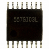
... IDT™ / ICS™ PCI-EXPRESS GEN1 CLOCK SOURCE Symbol Conditions Min. θ Still air JA θ 1 m/s air flow JA θ 3 m/s air flow JA θ JC Marking Diagram (ICS557GI-03 Marking Diagram (ICS557GI-03LF PCIE SSCG Typ. Max. Units ° C/W 78 ° C/W 70 ° C/W 68 ° C 557GI-03 ...
Page 9
ICS557-03 PCI-EXPRESS GEN1 CLOCK SOURCE Package Outline and Package Dimensions Package dimensions are kept current with JEDEC Publication No INDEX AREA Ordering Information Part / Order Number Marking 557G-03 See Page 8 557G-03T ...
Page 10
ICS557-03 PCI-EXPRESS GEN1 CLOCK SOURCE Innovate with IDT and accelerate your future networks. Contact: www.IDT.com For Sales 800-345-7015 408-284-8200 Fax: 408-284-2775 Corporate Headquarters Integrated Device Technology, Inc. www.idt.com © 2006 Integrated Device Technology, Inc. All rights reserved. Product specifications subject ...