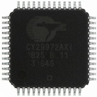
CY29972AXI Cypress Semiconductor Corp, CY29972AXI Datasheet - Page 5

CY29972AXI
Manufacturer Part Number
CY29972AXI
Description
IC CLK ZDB 12OUT 125MHZ 52TQFP
Manufacturer
Cypress Semiconductor Corp
Type
Fanout Distribution, Multiplexer , Spread Spectrum Clock Generator, Zero Delay Bufferr
Datasheet
1.CY29972AXI.pdf
(8 pages)
Specifications of CY29972AXI
Number Of Circuits
1
Package / Case
52-TQFP
Pll
Yes with Bypass
Input
Clock, Crystal
Output
Clock
Ratio - Input:output
4:12
Differential - Input:output
No/No
Frequency - Max
125MHz
Divider/multiplier
Yes/No
Voltage - Supply
2.9 V ~ 3.6 V
Operating Temperature
-40°C ~ 85°C
Mounting Type
Surface Mount
Frequency-max
125MHz
Maximum Input Frequency
480 MHz
Minimum Input Frequency
200 MHz
Output Frequency Range
125 MHz
Supply Voltage (max)
3.6 V
Supply Voltage (min)
2.9 V
Maximum Operating Temperature
+ 85 C
Minimum Operating Temperature
- 40 C
Mounting Style
SMD/SMT
Operating Supply Voltage
3.3 V
Lead Free Status / RoHS Status
Lead free / RoHS Compliant
Lead Free Status / RoHS Status
Lead free / RoHS Compliant, Lead free / RoHS Compliant
Other names
428-2236
CY29972AXI
CY29972AXI
Available stocks
Company
Part Number
Manufacturer
Quantity
Price
Company:
Part Number:
CY29972AXI
Manufacturer:
CY
Quantity:
4 918
Company:
Part Number:
CY29972AXI
Manufacturer:
Cypress Semiconductor Corp
Quantity:
10 000
Company:
Part Number:
CY29972AXIT
Manufacturer:
Cypress Semiconductor Corp
Quantity:
10 000
Part Number:
CY29972AXIT
Manufacturer:
CYPRESS
Quantity:
20 000
Document #: 38-07290 Rev. *C
Power Management
The individual output enable/freeze control of the CY29972
allows the user to implement unique power management
schemes into the design. The outputs are stopped in the logic
‘0’ state when the freeze control bits are activated. The serial
input register contains one programmable freeze enable bit for
12 of the 14 output clocks. The QC0 and FB_OUT outputs can
not be frozen with the serial port, this avoids any potential lock
up situation should an error occur in the loading of the serial
Table 3. Suggested Oscillator Crystal Parameters
Absolute Maximum Ratings
Maximum input voltage relative to V
Maximum input voltage relative to V
Storage temperature: .................................. –65°C to +150°C
Operating temperature:................................. –40°C to +85°C
Maximum ESD protection ................................................ 2kV
Maximum power supply: .................................................5.5V
Maximum input current: .............................................±20 mA
Note:
T
T
T
C
R
3. For best performance and accurate frequencies from this device, It is recommended but not mandatory that the chosen crystal meet or exceed these specifications.
4. Larger values may cause this device to exhibit oscillator start-up problems.
5. Multiple Supplies: The voltage on any input or I/O pin cannot exceed the power pin during power-up. Power supply sequencing is NOT required.
Parameter
C
S
A
L
ESR
Frequency Tolerance
Frequency Temperature Stability
Aging
Load Capacitance
Effective Series Resistance (ESR)
Characteristic
D0-D3 are the control bits for QA0-QA3, respectively
D4-D7 are the control bits for QB0-QB3, respectively
D8-D10 are the control bits for QC1-QC3, respectively
D11 is the control bit for SYNC
Start
SS
DD
Bit
[5]
: .............. V
: ............... V
D0 D1 D2 D3 D4 D5 D6 D7 D8 D9 D10 D11
DD
SS
Min.
– 0.3V
+ 0.3V
–
–
–
–
–
Figure 2.
Typ.
20
40
–
–
–
data. An output is frozen when a logic ‘0’ is programmed and
enabled when a logic ‘1’ is written. The enabling and freezing
of individual outputs is done in such a manner as to eliminate
the possibility of partial “runt” clocks.
The serial input register is programmed through the SDATA
input by writing a logic ‘0’ start bit followed by 12 NRZ freeze
enable bits. The period of each SDATA bit equals the period of
the free running SCLK signal. The SDATA is sampled on the
rising edge of SCLK.
This device contains circuitry to protect the inputs against
damage due to high static voltages or electric field; however,
precautions should be taken to avoid application of any
voltage higher than the maximum rated voltages to this circuit.
For proper operation, V
the range:
V
to an appropriate logic voltage level (either V
SS
< (V
Max.
±100
±100
IN
80
5
–
or V
OUT
) < V
PPM/Yr
Ohms
PPM
PPM
Unit
pF
DD .
IN
and V
Unused inputs must always be tied
Note 3
(T
(first 3 years @ 25°C)
The crystal’s rated load.
Note 4
OUT
A
–10 to +60°C)
should be constrained to
Conditions
SS
CY29972
or V
Page 5 of 8
[3]
DD
[3]
).
[3]
[+] Feedback


