ICS557G-03LF IDT, Integrated Device Technology Inc, ICS557G-03LF Datasheet - Page 6
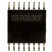
ICS557G-03LF
Manufacturer Part Number
ICS557G-03LF
Description
IC CLOCK SOURCE PCI 16-TSSOP
Manufacturer
IDT, Integrated Device Technology Inc
Type
Clock Generatorr
Specifications of ICS557G-03LF
Input
Clock, Crystal
Output
HCSL, LVDS
Frequency - Max
200MHz
Voltage - Supply
2.97 V ~ 3.63 V
Operating Temperature
0°C ~ 70°C
Mounting Type
Surface Mount
Package / Case
16-TSSOP
Frequency-max
200MHz
Number Of Elements
1
Supply Current
78mA
Pll Input Freq (min)
25MHz
Operating Supply Voltage (typ)
3.3V
Operating Temp Range
0C to 70C
Package Type
TSSOP
Output Frequency Range
25 to 200MHz
Operating Supply Voltage (min)
2.97V
Operating Supply Voltage (max)
3.63V
Operating Temperature Classification
Commercial
Pin Count
16
Lead Free Status / RoHS Status
Lead free / RoHS Compliant
Other names
557G-03LF
800-1062
800-1062-5
800-1062
800-1062
800-1062-5
800-1062
Available stocks
Company
Part Number
Manufacturer
Quantity
Price

Part Number:
ICS557G-03LF
Manufacturer:
ICS
Quantity:
20 000
Company:
Part Number:
ICS557G-03LFT
Manufacturer:
TOREX
Quantity:
500
Part Number:
ICS557G-03LFT
Manufacturer:
IDT
Quantity:
20 000
Part Number:
ICS557G-03LFTR
Manufacturer:
ICS
Quantity:
20 000


Absolute Maximum Ratings
DC Electrical Characteristics
IDT™ / ICS™ PCI-EXPRESS GEN1 CLOCK SOURCE
Supply Voltage
Input High Voltage
Input Low Voltage
Input Leakage Current
Operating Supply Current
Input Capacitance
Output Capacitance
Pin Inductance
Output Resistance
Pull-up Resistor
ICS557-03
PCI-EXPRESS GEN1 CLOCK SOURCE
Parameter
Stresses above the ratings listed below can cause permanent damage to the ICS557-03. These ratings are stress
ratings only. Functional operation of the device at these or any other conditions above those indicated in the
operational sections of the specifications is not implied. Exposure to absolute maximum rating conditions for
extended periods can affect product reliability. Electrical parameters are guaranteed only over the recommended
operating temperature range.
Unless stated otherwise, VDD = 3.3 V ±10%, Ambient Temperature -40 to +85° C
1. Single edge is monotonic when transitioning through region.
2. Inputs with pull-ups/-downs are not included.
Supply Voltage, VDDXD, VDDODA
All Inputs and Outputs
Ambient Operating Temperature (commercial)
Ambient Operating Temperature (industrial)
Storage Temperature
Junction Temperature
Soldering Temperature
ESD Protection (Input)
1
1
2
Symbo
I
C
R
DDOE
L
R
C
V
I
V
I
OUT
OUT
DD
PIN
V
IL
PU
l
IH
IL
IN
Item
S0, S1, OE, ICLK, SS0, SS1
S0, S1, OE, ICLK, SS0, SS1
0 < Vin < VDD
50Ω , 2 pF
OE =Low
Input pin capacitance
Output pin capacitance
CLK outputs
S0, S1, OE, SS0, SS1
Conditions
6
7 V
-0.5 V to VDD+0.5 V
0 to +70° C
-40 to +85° C
-65 to +150° C
125° C
260° C
2000 V min. (HBM)
VSS-0.3
Min.
2.97
2.0
3.0
-5
Typ.
100
3.3
Rating
VDD +0.3
Max.
3.63
0.8
78
44
5
7
6
5
ICS557-03
Units
mA
mA
nH
µA
pF
pF
kΩ
kΩ
V
V
V
PCIE SSCG
REV M 042709
Related parts for ICS557G-03LF
Image
Part Number
Description
Manufacturer
Datasheet
Request
R

Part Number:
Description:
IC CLK SOURCE QUAD PCI 20-TSSOP
Manufacturer:
IDT, Integrated Device Technology Inc
Datasheet:

Part Number:
Description:
IC CLK SOURCE QUAD DIFF 20-TSSOP
Manufacturer:
IDT, Integrated Device Technology Inc
Datasheet:

Part Number:
Description:
IC CLK BUFFER 1:4 HCSL 20-TSSOP
Manufacturer:
IDT, Integrated Device Technology Inc
Datasheet:

Part Number:
Description:
IC MUX 2:1 PCI-EXPRESS 16-TSSOP
Manufacturer:
IDT, Integrated Device Technology Inc
Datasheet:

Part Number:
Description:
IC CLK BUFFER 1:4 HCSL 20-TSSOP
Manufacturer:
IDT, Integrated Device Technology Inc
Datasheet:
Part Number:
Description:
IC CLK BUFFER 1:4 HCSL 20-TSSOP
Manufacturer:
IDT, Integrated Device Technology Inc
Datasheet:
Part Number:
Description:
IC MUX 2:1 PCI EXPRESS 16-TSSOP
Manufacturer:
IDT, Integrated Device Technology Inc
Datasheet:
Part Number:
Description:
IC MUX 2:1 PCI EXPRESS 16-TSSOP
Manufacturer:
IDT, Integrated Device Technology Inc
Datasheet:
Part Number:
Description:
IC CLK BUFFER 1:4 HCSL 20-TSSOP
Manufacturer:
IDT, Integrated Device Technology Inc
Datasheet:
Part Number:
Description:
IC MUX 2:1 PCI EXPRESS 16-TSSOP
Manufacturer:
IDT, Integrated Device Technology Inc
Datasheet:

Part Number:
Description:
IC CLK SOURCE PCI EXPRSS 16TSSOP
Manufacturer:
IDT, Integrated Device Technology Inc
Datasheet:
Part Number:
Description:
IC CLOCK SOURCE PCI EXP 16-TSSOP
Manufacturer:
IDT, Integrated Device Technology Inc
Datasheet:
Part Number:
Description:
IC CLOCK SOURCE PCI EXP 16-TSSOP
Manufacturer:
IDT, Integrated Device Technology Inc
Datasheet:
Part Number:
Description:
IC CLK SOURCE QUAD DIFF 20-TSSOP
Manufacturer:
IDT, Integrated Device Technology Inc
Datasheet:
Part Number:
Description:
IC CLK SOURCE QUAD DIFF 20-TSSOP
Manufacturer:
IDT, Integrated Device Technology Inc
Datasheet: