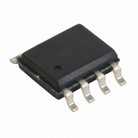
CY2305SXI-1 Cypress Semiconductor Corp, CY2305SXI-1 Datasheet - Page 4

CY2305SXI-1
Manufacturer Part Number
CY2305SXI-1
Description
IC CLK ZDB 5OUT 133MHZ 8SOIC
Manufacturer
Cypress Semiconductor Corp
Type
Fanout Distribution, Zero Delay Bufferr
Datasheet
1.CY2305SXC-1.pdf
(19 pages)
Specifications of CY2305SXI-1
Number Of Circuits
1
Package / Case
8-SOIC (3.9mm Width)
Pll
Yes
Input
LVCMOS, LVTTL
Output
LVCMOS
Ratio - Input:output
1:5
Differential - Input:output
No/No
Frequency - Max
133.33MHz
Divider/multiplier
No/No
Voltage - Supply
3 V ~ 3.6 V
Operating Temperature
-40°C ~ 85°C
Mounting Type
Surface Mount
Frequency-max
133MHz
Output Frequency Range
10 MHz to 133.33 MHz
Supply Voltage (max)
3.6 V
Supply Voltage (min)
3 V
Maximum Operating Temperature
+ 85 C
Minimum Operating Temperature
- 40 C
Mounting Style
SMD/SMT
Operating Supply Voltage
3.3 V
Lead Free Status / RoHS Status
Lead free / RoHS Compliant
Lead Free Status / RoHS Status
Lead free / RoHS Compliant, Lead free / RoHS Compliant
Other names
428-1792
CY2305SXI-1
CY2305SXI-1
Available stocks
Company
Part Number
Manufacturer
Quantity
Price
Part Number:
CY2305SXI-1
Manufacturer:
CYPRESS/赛普拉斯
Quantity:
20 000
Company:
Part Number:
CY2305SXI-1H
Manufacturer:
CY
Quantity:
706
Part Number:
CY2305SXI-1H
Manufacturer:
CYPRESS/赛普拉斯
Quantity:
20 000
Company:
Part Number:
CY2305SXI-1HT
Manufacturer:
CYPRESS34
Quantity:
150
Part Number:
CY2305SXI-1HT
Manufacturer:
CYPRESS/赛普拉斯
Quantity:
20 000
Part Number:
CY2305SXI-1T
Manufacturer:
CYPRESS/赛普拉斯
Quantity:
20 000
Table 2. Pin Description for CY2309
Select Input Decoding for CY2309
Zero Delay and Skew Control
All outputs must be uniformly loaded to achieve zero delay between the input and output. Because the CLKOUT pin is the internal
feedback to the PLL, its relative loading can adjust the input-output delay. This is shown in the above graph.
For applications requiring zero input-output delay, all outputs, including CLKOUT, must be equally loaded. Even if CLKOUT is not
used, it must have a capacitive load, equal to that on other outputs, for obtaining zero input-output delay. If input to output delay
adjustments are required, use
For zero output-output skew, be sure to load all outputs equally. For further information, refer to the application note titled
and CY2309 as PCI and SDRAM
Document Number : 38-07140 Rev. *M
Notes
4. Weak pull down on all outputs
5. This output is driven and has an internal feedback for the PLL. The load on this output can be adjusted to change the skew between the reference and output.
S2
0
0
1
1
Pin
13
14
15
16
Figure 3. REF. Input to CLKA/CLKB Delay vs. Loading Difference between CLKOUT and CLKA/CLKB Pins
S1
0
1
0
1
V
CLKA3
CLKA4
CLKOUT
DD
CLOCK A1–A4
Three-state
Driven
Driven
Driven
[4]
[4]
[4]
Signal
Figure 3
Buffers.”
CLOCK B1–B4
to calculate loading differences between the CLKOUT pin and other outputs.
Three-state
Three-state
Driven
Driven
3.3-V supply
Buffered clock output, Bank A
Buffered clock output, Bank A
Buffered output, internal feedback on this pin
CLKOUT
Driven
Driven
Driven
Driven
[5]
Description
Output Source
Reference
PLL
PLL
PLL
CY2305, CY2309
PLL Shutdown
N
N
N
Y
Page 4 of 19
“CY2305
[+] Feedback


