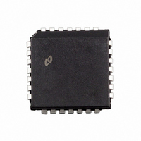
CGS2535V National Semiconductor, CGS2535V Datasheet - Page 3

CGS2535V
Manufacturer Part Number
CGS2535V
Description
IC CLOCK DVR COM QUAD 1-4 28PLCC
Manufacturer
National Semiconductor
Type
Fanout Buffer (Distribution)r
Datasheet
1.CGS2535TV.pdf
(7 pages)
Specifications of CGS2535V
Number Of Circuits
1
Ratio - Input:output
4:16
Differential - Input:output
No/No
Input
CMOS
Output
CMOS
Frequency - Max
125MHz
Voltage - Supply
3 V ~ 5.25 V
Operating Temperature
0°C ~ 70°C
Mounting Type
Surface Mount
Package / Case
28-PLCC
Frequency-max
125MHz
Lead Free Status / RoHS Status
Contains lead / RoHS non-compliant
Other names
*CGS2535V
Available stocks
Company
Part Number
Manufacturer
Quantity
Price
Company:
Part Number:
CGS2535V
Manufacturer:
NSC
Quantity:
5 510
Company:
Part Number:
CGS2535VX
Manufacturer:
NSC
Quantity:
540
Part Number:
CGS2535VX
Manufacturer:
NS/国半
Quantity:
20 000
f
t
t
t
t
t
t
t
t
t
t
t
t
t
t
t
t
t
t
Symbol
max
PLH
PHL
PLH
PHL
OSLH
OSHL
rise
fall
rise
fall
rise
fall
High
Low
PVLH
PVHL
PVLH
PVHL
AC Electrical Characteristics
Over recommended operating free air temperature specified. All typical values are measured at V
Note 4: Output-to-Output Skew is defined as the absolute value of the difference between the actual propagation delay for any outputs within the same packaged
device and output bank. The specifications apply to any outputs switching in the same direction either LOW to HIGH (t
Note 5: Time high is measured with outputs at 2.0V or above. Time low is measured with outputs at 0.8V or below. Input waveform characteristics for t
measurement: f = 66.67 MHz, duty cycle = 50%.
,
,
,
Frequency Maximum
Low-to-High Propagation Delay
CK to O
High-to-Low Propagation Delay
CK to O
Low-to-High Propagation Delay
CK to O
14)
High-to-Low Propagation Delay
CK to O
14)
Maximum Skew Common Edge
Output-to-Output Variation
(Note 4) (Note 6)
Maximum Skew Common Edge
Output-to-Output Variation
(Note 4) (Note 6)
Rise/Fall Time
(from 0.8V/2.0V to 2.0V/0.8V) (Note 8)
Rise/Fall Time
(from 0.8V/2.0V to 2.0V/0.8V) (Note 9)
(Note 14)
Rise/Fall Time
(from 0.8V/2.0V to 2.0V/0.8V) (Note 10)
(Note 14)
Pulse Width Duration High
(Note 5) (Note 6) (Note 14)
Pulse Width Duration Low
(Note 5) (Note 6) (Note 14)
Part-to-Part Variation of
Low-to-High Transitions
Part-to-Part Variation of
High-to-Low Transitions
Part-to-Part Variation of
Low-to-High Transitions
Part-to-Part Variation of
High-to-Low Transitions
@
@
@
@
1 MHz (Note 13)
1 MHz (Note 13)
66.67 MHz (Note 13) (Note 14)
66.67 MHz (Note 13) (Note 14)
n
n
n
n
@
@
@
@
1 MHz (Note 13)
1 MHz (Note 13)
66.67 MHz (Note 13) (Note
66.67 MHz (Note 13) (Note
Parameter
(Notes 4, 5, 6)
(Note 11)
V
(V)
3.0
5.0
3.3
5.0
3.3
5.0
3.3
5.0
3.3
5.0
3.3
5.0
3.3
5.0
3.3
5.0
3.3
5.0
3.3
5.0
3.3
5.0
3.3
5.0
3.3
5.0
3.3
5.0
3.3
5.0
3.3
5.0
CC
3
C
Min
4.0
4.0
4.0
4.0
L
= 50 pF, R
T
A
= +25˚C
Typ
150
150
150
150
L
= 500Ω
Max
350
350
350
350
650
650
650
650
4.5
3.5
4.5
3.5
5.0
4.5
5.0
4.5
3.5
3.0
0.8
0.4
1.0
0.7
1.0
1.0
1.0
1.0
CGS2535
OSLH
C
Min
T
2.5
2.0
2.5
2.0
2.5
2.0
2.5
2.0
4.0
4.0
4.0
4.0
L
) or HIGH to LOW (t
CC
A
= 50 pF, R
= −40˚C to +85˚C
= 5V, T
(Note 7)
Typ
100
125
300
300
300
300
A
L
= 25˚C.
= 500Ω
OSHL
Max
350
350
350
350
650
650
4.5
3.5
4.5
3.5
5.0
4.5
5.0
4.5
3.5
3.0
1.0
0.6
1.0
0.9
1.0
1.0
1.0
1.0
1.0
1.0
www.national.com
).
High
, t
Units
MHz
Low
ns
ns
ns
ns
ps
ps
ns
ns
ns
ns
ns
ps
ns
ps
ns


