NB7L111MMNG ON Semiconductor, NB7L111MMNG Datasheet - Page 3
NB7L111MMNG
Manufacturer Part Number
NB7L111MMNG
Description
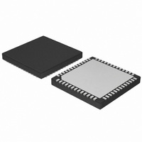
IC DRVR CLK/DATA 1:10 DIFF 52QFN
Manufacturer
ON Semiconductor
Type
Fanout Buffer (Distribution), Multiplexer , Datar
Datasheet
1.NB7L111MMNR2G.pdf
(13 pages)
Specifications of NB7L111MMNG
Number Of Circuits
1
Ratio - Input:output
2:10
Differential - Input:output
Yes/Yes
Input
CML, LVCMOS, LVDS, LVNECL, LVPECL, LVTTL
Output
CML
Frequency - Max
5.5GHz
Voltage - Supply
2.375 V ~ 3.465 V
Operating Temperature
-40°C ~ 85°C
Mounting Type
Surface Mount
Package / Case
52-VFQFN Exposed Pad
Frequency-max
5.5GHz
Output Logic Level
CML
Supply Voltage (max)
3.465 V
Supply Voltage (min)
2.375 V
Maximum Operating Temperature
+ 85 C
Maximum Data Rate
6 Gbps
Minimum Operating Temperature
- 40 C
Mounting Style
SMD/SMT
Number Of Clock Inputs
2
Supply Current
290 mA
Lead Free Status / RoHS Status
Lead free / RoHS Compliant
Available stocks
Company
Part Number
Manufacturer
Quantity
Price
Company:

Part Number:
NB7L111MMNG
Manufacturer:
ON Semiconductor
Quantity:
15
Part Number:
NB7L111MMNG
Manufacturer:
ON/安森美
Quantity:
20 000


1. CML output requires 50 W receiver termination resistor to V
2. In the differential configuration when the input termination pin (VTCLK, VTCLK) are connected to a common termination voltage or left open,
Table 2. PIN DESCRIPTION
17, 20, 23, 29, 32, 35,
16, 19, 22, 28, 31, 34,
15, 24, 27, 39, 42, 51
1, 18, 21, 26, 30, 33,
and if no signal is applied on CLK and CLK then the device will be susceptible to self−oscillation.
36, 40, 45, 48
14, 25, 41, 52
38, 44, 47, 50
37, 43, 46, 49
Pin
EP
10
11
12
13
2
3
4
5
6
7
8
9
VTCLK0
VTCLK0
VTCLK1
VTCLK1
VTSEL
VTSEL
Q[0−9]
Q[0−9]
Name
CLK0
CLK0
CLK1
CLK1
V
SEL
SEL
V
NC
CC
−
EE
LVCMOS, LVTTL,
LVCMOS, LVTTL,
LVCMOS, LVTTL,
LVCMOS, LVTTL,
LVCMOS, LVTTL,
LVCMOS, LVTTL,
LVCMOS, LVTTL,
LVPECL, CML,
LVPECL, CML,
LVPECL, CML,
LVPECL, CML,
LVPECL, CML,
LVPECL, CML,
LVPECL, CML,
CML Outputs
CML Outputs
LVDS Input
LVDS Input
LVDS Input
LVDS Input
LVDS Input
LVDS Input
LVDS Input
I/O
−
−
−
−
−
−
−
−
http://onsemi.com
CC
for proper operation.
Positive supply voltage. All V
power supply to guarantee proper operation.
Negative supply voltage. All V
power supply to guarantee proper operation.
Internal 50 W termination pin for CLK0. (Note 2)
Non−inverted differential clock/data input 0 (Note 2).
Inverted differential clock/data input 0 (Note 2).
Internal 50 W termination pin for CLK0. (Note 2)
Internal 50 W termination pin for SEL. (Note 2)
Non−inverted differential clock/data select input. Internal 75 kW to V
Inverted differential clock/data select input. Internal 56 KW to V
56 kW to V
Internal 50 W termination pin for SEL. (Note 2)
Internal 50 W termination pin for CLK1. (Note 2)
Non−inverted differential clock/data input 1 (Note 2).
Inverted differential clock/data input 1 (Note 2).
Internal 50 W termination pin for CLK1. (Note 2)
Non−inverted CML outputs [0−9] with internal 50 W source termination
resistor (Note 1).
Inverted CML outputs [0−9] with internal 50 W source termination
resistor (Note 1).
Exposed Pad (EP). The thermally exposed pad on package bottom (see
case drawing) must be attached to a heat−sinking conduit on the printed
circuit board.
3
EE
bias this pin to (V
CC
Description
EE
CC
pins must be externally connected to
pins must be externally connected to
−V
EE
)/2.
CC
and
EE
.
Related parts for NB7L111MMNG
Image
Part Number
Description
Manufacturer
Datasheet
Request
R

Part Number:
Description:
ON Semiconductor [VOLTAGE REGULATOR]
Manufacturer:
ON Semiconductor
Datasheet:
Part Number:
Description:
357-036-542-201 CARDEDGE 36POS DL .156 BLK LOPRO
Manufacturer:
ON Semiconductor
Datasheet:
Part Number:
Description:
357-036-542-201 CARDEDGE 36POS DL .156 BLK LOPRO
Manufacturer:
ON Semiconductor
Datasheet:
Part Number:
Description:
357-036-542-201 CARDEDGE 36POS DL .156 BLK LOPRO
Manufacturer:
ON Semiconductor
Datasheet:
Part Number:
Description:
357-036-542-201 CARDEDGE 36POS DL .156 BLK LOPRO
Manufacturer:
ON Semiconductor
Datasheet:
Part Number:
Description:
357-036-542-201 CARDEDGE 36POS DL .156 BLK LOPRO
Manufacturer:
ON Semiconductor
Datasheet:
Part Number:
Description:
357-036-542-201 CARDEDGE 36POS DL .156 BLK LOPRO
Manufacturer:
ON Semiconductor
Datasheet:
Part Number:
Description:
357-036-542-201 CARDEDGE 36POS DL .156 BLK LOPRO
Manufacturer:
ON Semiconductor
Datasheet:
Part Number:
Description:
357-036-542-201 CARDEDGE 36POS DL .156 BLK LOPRO
Manufacturer:
ON Semiconductor
Datasheet:
Part Number:
Description:
357-036-542-201 CARDEDGE 36POS DL .156 BLK LOPRO
Manufacturer:
ON Semiconductor
Datasheet:
Part Number:
Description:
357-036-542-201 CARDEDGE 36POS DL .156 BLK LOPRO
Manufacturer:
ON Semiconductor
Datasheet:
Part Number:
Description:
Manufacturer:
ON Semiconductor
Datasheet:
Part Number:
Description:
Manufacturer:
ON Semiconductor
Datasheet:
Part Number:
Description:
Manufacturer:
ON Semiconductor
Datasheet: