NB6N14SMNG ON Semiconductor, NB6N14SMNG Datasheet
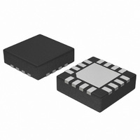
IC CLK/DATA RCVR DIFF 1:4 16-QFN

NB6N14SMNG

Manufacturer Part Number
NB6N14SMNG
Description
IC CLK/DATA RCVR DIFF 1:4 16-QFN
Manufacturer
ON Semiconductor
Series
AnyLevel™ ECLinPS MAX™r
Type
Fanout Buffer (Distribution), Translatorr
Datasheet

Specifications of NB6N14SMNG

Number Of Circuits
1
Ratio - Input:output
1:4
Differential - Input:output
Yes/Yes
Input
CML, LVDS, LVPECL
Output
LVDS
Frequency - Max
2GHz
Voltage - Supply
3 V ~ 3.6 V
Operating Temperature
-40°C ~ 85°C
Mounting Type
Surface Mount
Package / Case
16-TFQFN Exposed Pad
Frequency-max
2GHz
Number Of Outputs
8
Max Input Freq
2000 MHz (Min)
Propagation Delay (max)
0.6 ns @ 3V to 3.6V
Supply Voltage (max)
3.6 V
Supply Voltage (min)
3 V
Maximum Operating Temperature
+ 85 C
Minimum Operating Temperature
- 40 C
Mounting Style
SMD/SMT
Lead Free Status / RoHS Status
Lead free / RoHS Compliant
Other names
NB6N14SMNG
NB6N14SMNGOS

Available stocks

Company
Part Number
Manufacturer
Quantity
Price
Part Number:
NB6N14SMNG
Manufacturer:
ON
Quantity:
760
Part Number:
NB6N14SMNG
Manufacturer:
ON
Quantity:
298
NB6N14S
3.3 V 1:4 AnyLevelt
Differential Input to LVDS
Fanout Buffer/Translator
accept AnyLevelt differential input signals: LVPECL, CML or
LVDS. These signals will be translated to LVDS and four identical
copies of Clock or Data will be distributed, operating up to 2.0 GHz or
2.5 Gb/s, respectively. As such, the NB6N14S is ideal for SONET,
GigE, Fiber Channel, Backplane and other Clock or Data distribution
applications.
GND + 50 mV to V
termination resistors at the inputs, the NB6N14S is ideal for
translating a variety of differential or single−ended Clock or Data
signals to 350 mV typical LVDS output levels.
package. Application notes, models, and support documentation are
available at www.onsemi.com.
performance products.
Features
© Semiconductor Components Industries, LLC, 2009
April, 2009 − Rev. 6
The NB6N14S is a differential 1:4 Clock or Data Receiver and will
The NB6N14S has a wide input common mode range from
The NB6N14S is offered in a small 3 mm x 3 mm 16−QFN
The NB6N14S is a member of the ECLinPS MAXt family of high
SG Devices
Maximum Input Clock Frequency > 2.0 GHz
Maximum Input Data Rate > 2.5 Gb/s
1 ps Maximum RMS Clock Jitter
Typically 10 ps Data Dependent Jitter
380 ps Typical Propagation Delay
120 ps Typical Rise and Fall Times
V
TIA/EIA − 644 Compliant
Functionally Compatible with Existing 3.3 V LVEL, LVEP, EP, and
These are Pb−Free Devices
REF_AC
PRBS 2
Figure 2. Typical Output Waveform at 2.488 Gb/s with
Reference Output
23−1
(V
CC
INPP
− 50 mV. Combined with the 50 W internal
Device DDJ = 10 ps
= 400 mV; Input Signal DDJ = 14 ps)
TIME (58 ps/div)
1
See detailed ordering and shipping information in the package
dimensions section on page 10 of this data sheet.
VT
/IN
IN
(LVTTL/CMOS)
EN
*For additional marking information, refer to
CASE 485G
MN SUFFIX
(Note: Microdot may be in either location)
Application Note AND8002/D.
50
50
QFN−16
1
W
W
V
ORDERING INFORMATION
REF_AC
Figure 1. Logic Diagram
A = Assembly Location
L = Wafer Lot
Y = Year
W = Work Week
G = Pb−Free Package
http://onsemi.com
D
Publication Order Number:
1
Q
DIAGRAM*
16
MARKING
ALYW G
NB6N
14S
G
NB6N14S/D
Q0
Q0
Q1
Q1
Q2
Q2
Q3
Q3

Related parts for NB6N14SMNG

NB6N14SMNG Summary of contents

Page 1

NB6N14S 3.3 V 1:4 AnyLevelt Differential Input to LVDS Fanout Buffer/Translator The NB6N14S is a differential 1:4 Clock or Data Receiver and will accept AnyLevelt differential input signals: LVPECL, CML or LVDS. These signals will be translated to LVDS and ...

Page 2

GND NB6N14S Figure 3. NB6N14S Pinout, 16−pin QFN Table 2. PIN DESCRIPTION Pin Name I/O ...

Page 3

Table 3. ATTRIBUTES Moisture Sensitivity (Note 3) Flammability Rating ESD Protection Transistor Count Meets or exceeds JEDEC Spec EIA/JESD78 IC Latchup Test 3. For additional information, see Application Note AND8003/D. Table 4. MAXIMUM RATINGS Symbol Parameter V Positive Power Supply ...

Page 4

Table 5. DC CHARACTERISTICS V Symbol Characteristic I Power Supply Current (Note 9) CC DIFFERENTIAL INPUTS DRIVEN SINGLE−ENDED (Figures 14, 15, 19, and 21) V Input Threshold Reference Voltage Range (Note Single−ended Input HIGH Voltage IH V ...

Page 5

Table 6. AC CHARACTERISTICS V Symbol Characteristic f Maximum Input Clock Frequency inMax V Output Voltage Amplitude (@ V OUTPP (Figure 4) f Maximum Operating Data Rate DATA t , Differential Input to Differential Output PLH t Propagation Delay PHL ...

Page 6

Figure 5. Typical Phase Noise Plot 156.25 MHz carrier Figure 7. Typical Phase Noise Plot GHz carrier The above phase noise plots captured using Agilent E5052A show additive phase noise of the NB6N14S ...

Page 7

Device DDJ = 10 ps TIME (58 ps/div) Figure 9. Typical Output Waveform at 2.488 Gb/s with PRBS 100 mV; Input Signal DDJ = 14 ps) INPP http://onsemi.com 23−1 and OC48 mask 7 ...

Page 8

V CC NB6N14S CLK − 2 LVPECL Driver CLK V EE Figure 10. LVPECL Interface V CC NB6N14S CLK o ...

Page 9

LVDS Driver Device Figure 17. Typical LVDS Termination for Output Driver and Device Evaluation Figure 19. Differential Input Driven Single−Ended IHmax V thmax ...

Page 10

... /IN V INPP ORDERING INFORMATION Device NB6N14SMNG QFN−16 NB6N14SMNR2G QFN−16 †For information on tape and reel specifications, including part orientation and tape sizes, please refer to our Tape and Reel Packaging Specifications Brochure, BRD8011/ Figure 23. EN Timing Diagram Package (Pb−Free) (Pb−Free) http://onsemi.com ...

Page 11

... Pb−Free strategy and soldering details, please download the ON Semiconductor Soldering and Mounting Techniques Reference Manual, SOLDERRM/D. N. American Technical Support: 800−282−9855 Toll Free USA/Canada Europe, Middle East and Africa Technical Support: Phone: 421 33 790 2910 Japan Customer Focus Center Phone: 81− ...

Related keywords