NB4N121KMNG ON Semiconductor, NB4N121KMNG Datasheet - Page 5
NB4N121KMNG
Manufacturer Part Number
NB4N121KMNG
Description
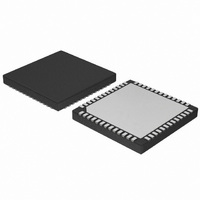
IC FANOUT CLK DRVR HCSL 52-QFN
Manufacturer
ON Semiconductor
Type
Fanout Buffer (Distribution)r
Datasheet
1.NB4N121KMNR2G.pdf
(9 pages)
Specifications of NB4N121KMNG
Number Of Circuits
1
Ratio - Input:output
1:21
Differential - Input:output
Yes/Yes
Input
CML, LVCMOS, LVDS, LVPECL, LVTTL
Output
HCSL
Frequency - Max
400MHz
Voltage - Supply
3 V ~ 3.6 V
Operating Temperature
-40°C ~ 70°C
Mounting Type
Surface Mount
Package / Case
52-VFQFN Exposed Pad
Frequency-max
400MHz
Lead Free Status / RoHS Status
Lead free / RoHS Compliant
Available stocks
Company
Part Number
Manufacturer
Quantity
Price
Company:

Part Number:
NB4N121KMNG
Manufacturer:
ON Semiconductor
Quantity:
95
Part Number:
NB4N121KMNG
Manufacturer:
ON/安森美
Quantity:
20 000


NOTE: Device will meet the specifications after thermal equilibrium has been established when mounted in a test socket or printed circuit
7. Measured by forcing V
8. Measured from the input pair crosspoint to each single output pair crosspoint across temp and voltage ranges.
9. Duty cycle skew is measured between differential outputs using the deviations of the sum of Tpw− and Tpw+.
10. Skew is measured between outputs under identical transition @ 133 MHz.
11. Additive RMS jitter with 50% duty cycle clock signal using phase noise integrated from 12 KHz to 33 MHz
Table 5. AC CHARACTERISTICS
Symbol
V
t
t
Dt
Dt
t
t
V
DV
t
Dt
PLH
PHL
SKEW
JITTER
r
, t
OUTPP
cross
to GND) or 2X (all outputs loaded 25 W to GND) configuration, see Figure 9. For 1X configuration, connect I
configuration, connect I
PLH
PHL
r,
cross
f
Dt
,
,
f
board with maintained transverse airflow greater than 500 lfpm. Electrical parameters are guaranteed only over the declared
operating temperature range. Functional operation of the device exceeding these conditions is not implied. Device specification limit
values are applied individually under normal operating conditions and not valid simultaneously.
Output Voltage Amplitude (@ V
Propagation Delay to (See Figure 3)
Propagation Delay Variations Variation Per Each Diff Pair CLK/CLK to Qx/Qx (Note 8)
(See Figure 3)
Duty Cycle Skew (Note 9)
Within−Device Skew, 1X Mode Only (Note 10)
Within−Device Skew, 2X Mode (Note 10)
Device−to−Device Skew (Note 10)
RMS Random Clock Jitter (Note 11)
Absolute Crossing Magnitude Voltage
Variation in Magnitude of V
Absolute Magnitude in Output Risetime and Falltime
(From 175 mV to 525 mV)
Variation in Magnitude of Risetime and Falltime (Single−Ended)
(See Figure 4)
INPP
REF
(MIN) from a 50% duty cycle clock source. Measurements taken with outputs in either 1X (all outputs loaded 50 W
to V
CC
. Typical gain is 20 dB.
cross
CLK
CLK
V
CC
INPPmin
= 3.0 V to 3.6 V, GND = 0 V; −40°C to +70°C (Note 7)
Figure 3. AC Reference Measurement
Characteristic
Q
Q
)
Dt
PLH
http://onsemi.com
t
PLH
5
t
PHL
CLK/CLK to Qx/Qx
V
INPP
f
f
f
f
f
in
in
in
in
in
f
in
= V
= V
V
= 133 MHz
= 166 MHz
= 200 MHz
= 166 MHz
= 200 MHz
=133 MHz
OUTPP
IH
IH
Dt
Qx, Qx
Qx, Qx
(CLK) − V
(CLK) − V
PHL
1X
2X
= V
= V
OH
OH
IL
IL
Min
(Q) − V
(Q) − V
550
250
175
(CLK)
(CLK)
OL
OL
(Q)
(Q)
Typ
725
725
725
800
340
REF
to GND, or for 2X
Max
900
900
900
950
100
150
550
150
700
125
150
20
50
80
1
Unit
mV
mV
mV
ps
ps
ps
ps
ps
ps
ps
ps
ps
Related parts for NB4N121KMNG
Image
Part Number
Description
Manufacturer
Datasheet
Request
R

Part Number:
Description:
ON Semiconductor [VOLTAGE REGULATOR]
Manufacturer:
ON Semiconductor
Datasheet:
Part Number:
Description:
357-036-542-201 CARDEDGE 36POS DL .156 BLK LOPRO
Manufacturer:
ON Semiconductor
Datasheet:
Part Number:
Description:
357-036-542-201 CARDEDGE 36POS DL .156 BLK LOPRO
Manufacturer:
ON Semiconductor
Datasheet:
Part Number:
Description:
357-036-542-201 CARDEDGE 36POS DL .156 BLK LOPRO
Manufacturer:
ON Semiconductor
Datasheet:
Part Number:
Description:
357-036-542-201 CARDEDGE 36POS DL .156 BLK LOPRO
Manufacturer:
ON Semiconductor
Datasheet:
Part Number:
Description:
357-036-542-201 CARDEDGE 36POS DL .156 BLK LOPRO
Manufacturer:
ON Semiconductor
Datasheet:
Part Number:
Description:
357-036-542-201 CARDEDGE 36POS DL .156 BLK LOPRO
Manufacturer:
ON Semiconductor
Datasheet:
Part Number:
Description:
357-036-542-201 CARDEDGE 36POS DL .156 BLK LOPRO
Manufacturer:
ON Semiconductor
Datasheet:
Part Number:
Description:
357-036-542-201 CARDEDGE 36POS DL .156 BLK LOPRO
Manufacturer:
ON Semiconductor
Datasheet:
Part Number:
Description:
357-036-542-201 CARDEDGE 36POS DL .156 BLK LOPRO
Manufacturer:
ON Semiconductor
Datasheet:
Part Number:
Description:
357-036-542-201 CARDEDGE 36POS DL .156 BLK LOPRO
Manufacturer:
ON Semiconductor
Datasheet:
Part Number:
Description:
Manufacturer:
ON Semiconductor
Datasheet:
Part Number:
Description:
Manufacturer:
ON Semiconductor
Datasheet:
Part Number:
Description:
Manufacturer:
ON Semiconductor
Datasheet: