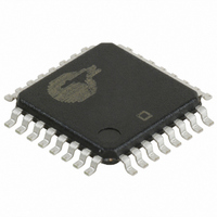
CY29940AXC Cypress Semiconductor Corp, CY29940AXC Datasheet - Page 2

CY29940AXC
Manufacturer Part Number
CY29940AXC
Description
IC CLK BUFF 1:18 200MHZ 32LQFP
Manufacturer
Cypress Semiconductor Corp
Type
Fanout Buffer (Distribution), Multiplexerr
Datasheet
1.CY29940AXI.pdf
(7 pages)
Specifications of CY29940AXC
Package / Case
32-LQFP
Number Of Circuits
1
Ratio - Input:output
1:18
Differential - Input:output
Yes/No
Input
LVCMOS, LVPECL, LVTTL
Output
LVCMOS, LVTTL
Frequency - Max
200MHz
Voltage - Supply
2.375 V ~ 3.465 V
Operating Temperature
0°C ~ 70°C
Mounting Type
Surface Mount
Frequency-max
200MHz
Minimum Operating Temperature
0 C
Mounting Style
SMD/SMT
Multiply / Divide Factor
1:18
Number Of Clock Inputs
2
Output Logic Level
LVCMOS, LVTTL
Supply Voltage (max)
3.465 V
Supply Voltage (min)
2.375 V
Maximum Operating Temperature
+ 70 C
Lead Free Status / RoHS Status
Lead free / RoHS Compliant
Lead Free Status / RoHS Status
Lead free / RoHS Compliant, Lead free / RoHS Compliant
Available stocks
Company
Part Number
Manufacturer
Quantity
Price
Company:
Part Number:
CY29940AXC
Manufacturer:
Cypress
Quantity:
359
Company:
Part Number:
CY29940AXC
Manufacturer:
CYPRESS
Quantity:
648
Company:
Part Number:
CY29940AXC
Manufacturer:
Cypress Semiconductor Corp
Quantity:
10 000
Company:
Part Number:
CY29940AXC-1
Manufacturer:
Cypress Semiconductor Corp
Quantity:
10 000
Company:
Part Number:
CY29940AXC-1T
Manufacturer:
Cypress Semiconductor Corp
Quantity:
10 000
Company:
Part Number:
CY29940AXCT
Manufacturer:
Cypress Semiconductor Corp
Quantity:
10 000
Part Number:
CY29940AXCT
Manufacturer:
CYPRESS/赛普拉斯
Quantity:
20 000
Document #: 38-07283 Rev. *D
Maximum Ratings
Maximum Input Voltage Relative to V
Maximum Input Voltage Relative to V
Storage Temperature: ................................ –65°C to + 150°C
Operating Temperature: ................................ –40°C to +85°C
Maximum ESD Protection............................................... 2 kV
Maximum Power Supply: ................................................5.5V
Maximum Input Current: ............................................±20 mA
DC Parameters
Notes:
2.
3.
4.
5.
6.
7.
V
V
I
I
V
V
V
V
I
I
Z
C
IL
IH
DDQ
DD
Parameter
IL
IH
PP
CMR
OL
OH
out
in
Multiple Supplies: The Voltage on any input or I/O pin cannot exceed the power pin during power-up. Power supply sequencing is NOT required.
Inputs have pull-up/pull-down resistors that effect input current.
The VCMR is the difference from the most positive side of the differential input signal. Normal operation is obtained when the “High” input is within the VCMR
range and the input lies within the VPP specification. Driving series or parallel terminated 50Ω (or 50Ω to VDD/2) transmission lines
Outputs driving 50Ω transmission lines.
See Figure 1 &2.
50% input duty cycle.
Input Low Voltage
Input High Voltage
Input Low Current
Input High Current
Peak-to-Peak Input
Voltage
PECL_CLK
Common Mode Range
PECL_CLK
Output Low Voltage
Output High Voltage
Quiescent Supply
Current
Dynamic Supply
Current
Output Impedance
Input Capacitance
[2]
:
V
[2]
DD
Description
= 3.3V ±5% or 2.5V ±5%, V
[3]
[3]
[5, 6, 7]
SS
DD
[5, 6, 7]
: ............ V
: ............. V
[4]
DD
SS
V
V
I
I
I
V
CL = 15 pF
V
CL = 15 pF
V
CL = 15 pF
V
CL = 15 pF
V
V
OL
OH
OH
DD
DD
DD
DD
DD
DD
DD
DD
– 0.3V
+ 0.3V
= 20 mA
DDC
= –20 mA, V
= –20 mA, V
= 3.3V, Outputs @ 150 MHz,
= 3.3V, Outputs @ 200 MHz,
= 2.5V, Outputs @ 150 MHz,
= 2.5V, Outputs @ 200 MHz,
= 3.3V
= 2.5V
= 3.3V
= 2.5V
= 3.3V ±5% or 2.5V ±5%, T
Conditions
This device contains circuitry to protect the inputs against
damage due to high static voltages or electric field; however,
precautions should be taken to avoid application of any volt-
age higher than the maximum rated voltages to this circuit. For
proper operation, V
range:
V
Unused inputs must always be tied to an appropriate logic volt-
age level (either V
SS
DDC
DDC
< (V
= 3.3V
= 2.5V
in
or V
out
) < V
SS
in
V
V
or V
A
and V
DD
DD
DD
Min.
V
500
= –40°C to +85°C
2.0
2.4
1.8
10
–
–
–
–
–
–
8
–
SS
DD
– 1.4
– 1.0
).
out
should be constrained to the
Typ.
285
335
200
240
12
15
–
–
–
–
–
–
–
–
–
–
5
4
V
V
DD
DD
CY29940
Max.
–200
1000
V
200
0.8
0.5
16
20
DD
–
–
7
–
–
–
–
–
– 0.6
– 0.6
Page 2 of 7
Unit.
mV
mA
mA
µA
µA
pF
V
V
V
V
V
V
V
Ω
[+] Feedback


